Semiconductor device manufacturing apparatus and operating method thereof

a technology of semiconductor devices and manufacturing apparatus, which is applied in the direction of electrical devices, chemistry apparatus and processes, cleaning processes and apparatus, etc., can solve the problems of large resistance value between copper wiring and copper electrodes, corrosion theory, and difficulty in forming an airtight connection structure between the container and the pipe,

Inactive Publication Date: 2006-12-28
TOKYO ELECTRON LTD
View PDF3 Cites 4 Cited by
  • Summary
  • Abstract
  • Description
  • Claims
  • Application Information

AI Technical Summary

Benefits of technology

[0010] The present invention provides a semiconductor device manufacturing apparatus and an operating method thereof in which metal contamination of an object to be processed caused by a metal component dissolved in a corrosive liquid source can be prevented in the semiconductor device manufacturing apparatus which performs a process by supplying a vapor of the corrosive liquid source to a processing container.
[0020] The protection current is supplied by a DC power source whose negative electrode is connected to the storing container and whose positive electrode is connected to an electrode a part of which is immersed in the corrosive liquid source in the storing container. Or the protection current is a current applied between an electrode and the storing container in which a part of the electrode is immersed in the corrosive liquid source in the storing container, where a main material of the electrode is a metal whose ionization tendency is greater than that of the metal of the storing container and the metal of the electrode, which metal does not damage the semiconductor device, by utilizing the difference of the ionization tendencies between the storing container and the electrode.
[0021] According to embodiments of the present invention, since a protection current applies to a storing container, made of a metal, which stores a corrosive liquid source, a metal component of the storing container can be prevented from being dissolved in the corrosive liquid source. Consequently, since the metal component is prevented from entering a processing container with a vapor of the corrosive liquid source, metal contamination of a semiconductor device caused by the metal component can be prevented. When an external power source method which runs a current between an insoluble electrode and the storing container is used, since the dissolution of the metal does not substantially occur, the metal contamination of the semiconductor device can be surely prevented. In addition, when an anodic protection method is used, a potential difference between a metal of the storing container and a metal whose ionization tendency is greater than that of the metal of the storing container, and a metal component of the electrode is dissolved; however, since a metal which does not damage the semiconductor device can be selected as the metal of the electrode, the same effect as described above can be obtained.

Problems solved by technology

However, when the via hole is filled by the copper electrode in this state, the resistance value between the copper wiring and the copper electrode becomes large.
If quartz or resin is used for the container, it is difficult to form an airtight connecting structure between the container and a pipe used for supplying the formic acid, because the pipe is generally made of metal.
When the metal potential is greater than the equilibrium potential E, corrosion theoretically occurs due to the progress of the ionization of the metal.
Consequently, metal contamination occurs in the semiconductor wafer.
Consequently, the yield of a semiconductor device may be decreased by the metal contamination.
With this, the metal component is absorbed by another semiconductor device manufacturing apparatus and the metal contamination occurs in the semiconductor wafer.

Method used


Image

  • Semiconductor device manufacturing apparatus and operating method thereof
  • Semiconductor device manufacturing apparatus and operating method thereof
  • Semiconductor device manufacturing apparatus and operating method thereof

Examples


Embodiment Construction

[0029] Referring now to the drawings, embodiments of the present invention are described.

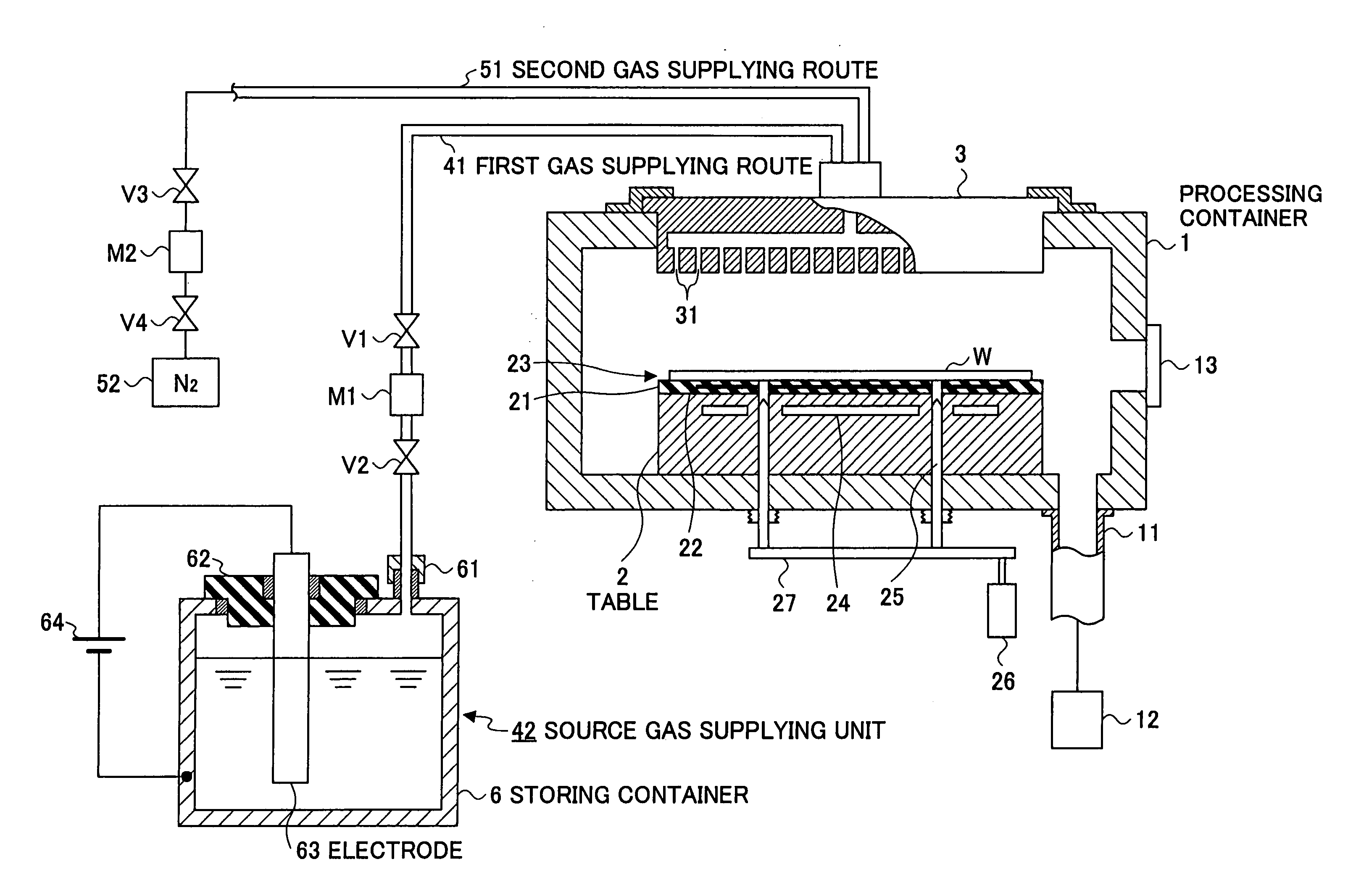
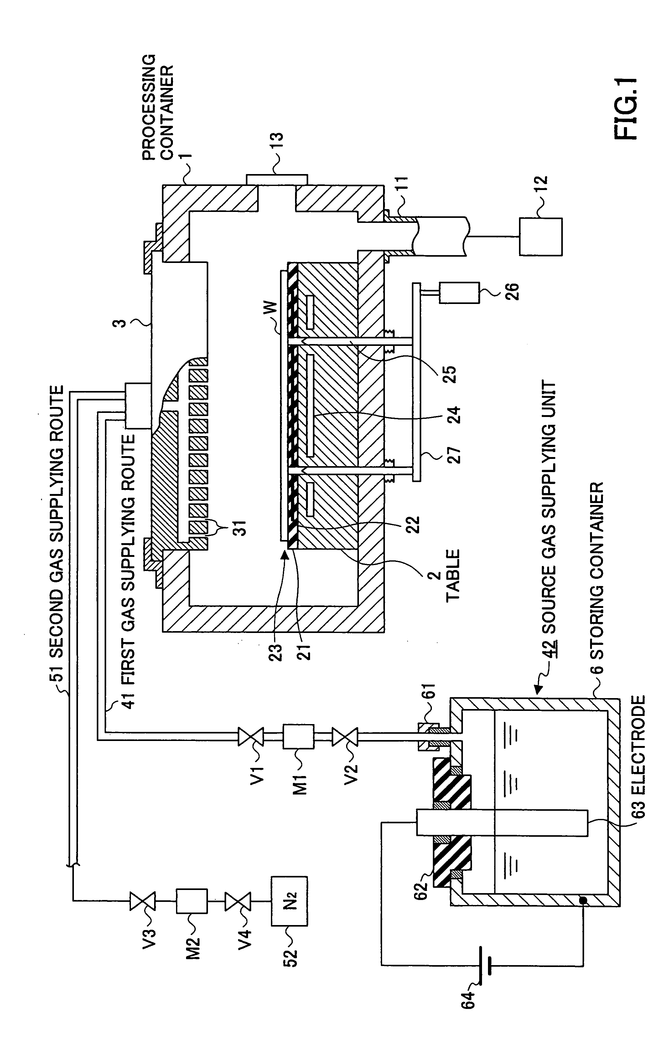
[0030]FIG. 1 is a structural diagram of a semiconductor device manufacturing apparatus according to an embodiment of the present invention. In FIG. 1, a processing container 1 which is a vacuum chamber is made of, for example, aluminum. A table 2, on which a semiconductor wafer W (an object to be processed) from which a semiconductor device is formed is put, is disposed on the bottom surface of the processing container 1. On the surface of the table 2, an electrostatic chuck 23 which is formed by embedding a chuck electrode 22 in a dielectric layer 21 is disposed, and a chuck voltage is applied to the electrostatic chuck 23 from a power source (not shown). In the table 2, a heater 24 which is a temperature adjusting unit is disposed, and a lifting pin 25 is disposed movably in the up and down directions to receive and send the semiconductor wafer W. A driving section 26 operates the lifting pin...


PUM

PropertyMeasurementUnit
pressureaaaaaaaaaa
voltageaaaaaaaaaa
corrosiveaaaaaaaaaa

Abstract

A semiconductor device manufacturing apparatus is disclosed. The semiconductor device manufacturing apparatus applies a process to a semiconductor wafer by supplying a vapor of a corrosive liquid source to a processing container. An electrode is immersed in a storing container which stores the corrosive liquid source. The main material of the electrode is a metal whose ionization tendency is less than that of a metal of the storing container, and a protection current is applied between them by a DC power source. Or another electrode is used. The main material of the electrode is a metal whose ionization tendency is greater than that of the metal of the storing container and the metal of the electrode does not damage the semiconductor wafer. A protection current is applied between the storing container and the electrode by utilizing the difference of the ionization tendency between them.

Description

BACKGROUND OF THE INVENTION [0001] 1. Field of the Invention [0002] The present invention relates to a semiconductor device manufacturing apparatus and an operating method thereof in which a process is applied to an object to be processed, for example, a reduction process is applied to a metal oxide, or a cleaning process is applied to the inside of a processing container, by supplying a vapor of a corrosive liquid source to the processing container. [0003] 2. Description of the Related Art [0004] There is a case where a process is performed by using a vapor of a corrosive liquid source in a semiconductor device manufacturing apparatus which provides a processing container so as to apply a process to a substrate. As an example, there is a process which reduces a surface oxide layer of copper wiring by using an organic acid. This process is described in detail. When copper multi-layer wiring is formed, in order to connect a lower copper layer to an upper copper layer, a via hole is f...

Claims


Application Information

Patent Timeline
Patent Type & Authority Applications(United States)
IPC IPC(8): C23F13/00
CPCB08B7/00H01L21/76814C23F13/02C23F13/00
Inventor MIYOSHI, HIDENORI
Owner TOKYO ELECTRON LTD
Why Eureka
Try Eureka