Unlock instant, AI-driven research and patent intelligence for your innovation.

Electro-optical device, electro-optical device driving method, image processing circuit, image processing method, and electronic apparatus

a technology of electrooptical devices and driving methods, applied in the direction of instruments, color signal processing circuits, visual presentations, etc., can solve the problems of reducing the memory capacity by half, and not meeting the recent demands for cost reduction, and achieve the effect of simplifying configuration and configuration

Inactive Publication Date: 2010-09-14
138 EAST LCD ADVANCEMENTS LTD
View PDF12 Cites 1 Cited by
  • Summary
  • Abstract
  • Description
  • Claims
  • Application Information

AI Technical Summary

Benefits of technology

"The invention provides an electro-optical device with a simplified configuration for storing and reading image data. The device includes a memory that stores upper n bits of image data, reads the stored n bits, and adds lower (m−n) bits to the n bits. A selecting circuit selects the input image data or the image data with the added bits. A scanning line driving circuit selects the scanning line corresponding to the selected image data. A data line driving circuit supplies the data signal converted by a converter to the data line corresponding to the selected image data. The invention also includes an image processing circuit and an electronic apparatus including the electro-optical device. The technical effect of the invention is to simplify the configuration of the device and reduce the amount of memory required."

Problems solved by technology

However, only reducing the memory capacity used by half does not satisfy recent demands for cost reduction.

Method used


Image

  • Electro-optical device, electro-optical device driving method, image processing circuit, image processing method, and electronic apparatus
  • Electro-optical device, electro-optical device driving method, image processing circuit, image processing method, and electronic apparatus
  • Electro-optical device, electro-optical device driving method, image processing circuit, image processing method, and electronic apparatus

Examples


Embodiment Construction

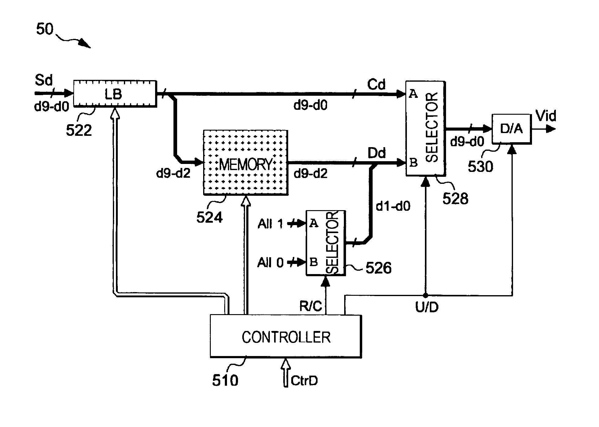
[0027]Embodiments of the invention will now be described with reference to the drawings. FIG. 1 is a block diagram showing an example of the configuration of an electro-optical device 10 according to an embodiment of the invention.

[0028]Referring to FIG. 1, the electro-optical device 10 includes a data processing circuit 50, a timing control circuit 60, a display area 100, a scanning line driving circuit 130, a sampling signal output circuit 140, sampling switches 150, and the like.

[0029]In the display area 100, 480 scanning lines 112 are arranged along an X direction, and 640 data lines 114 are arranged along a Y direction. Pixels 110 are arranged in association with intersections of the scanning lines 112 and the data lines 114. Thus, in this embodiment, the pixels 110 are arranged in matrix of 480 rows and 640 columns. However, the pixels 110 are not necessarily disposed in this arrangement.

[0030]The configuration of the pixels 110 will now be described. FIG. 2 shows an example o...


PUM


Abstract

An electro-optical device includes a plurality of pixels arranged in association with intersections of a plurality of scanning lines and a plurality of data lines, each of the plurality of pixels displaying a grayscale level corresponding to a data signal supplied to a corresponding data line when a scanning line is selected; a memory that stores upper n bits of input image data in which the grayscale level of each of the plurality of pixels is designated by m bits and that reads the stored n bits of image data, where “m” and “n ” represent positive integers satisfying a condition m>n; an adding circuit that adds lower (m−n) bits to the n bits of image data read from the memory; a selector that selects the input image data when the m bits of image data are input and that selects image data including the (m−n) bits added thereto by the adding circuit when the n bits of image data are read from the memory; a scanning line driving circuit that selects, from among the plurality of scanning lines, the scanning line corresponding to the image data selected by the selector; and a data line driving circuit that supplies the data signal based on the image data selected by the selector to the data line corresponding to the selected image data.

Description

BACKGROUND[0001]1. Technical Field[0002]The present invention relates to electro-optical devices that perform display in accordance with supplied image data, electro-optical device driving methods, image processing circuits, image processing methods, and electronic apparatuses.[0003]2. Related Art[0004]For display devices, it is important to make flickering less noticeable. In order to reduce flickering, for example, a technology described in Japanese Patent No. 2605261 (see FIG. 2) is suggested. In this technology, after image data for one frame is stored in first and second memories, the image data is read with a half-reduced horizontal scanning period. Thus, images for a period of two fields for interlaced scanning are converted into images for line sequential scanning by being compressed into images for a period of one frame (about 17 milliseconds).[0005]In this technology, a memory with a sufficient capacity for storing two pieces of image data for one field, that is, image dat...

Claims


Application Information

Patent Timeline
Patent Type & Authority Patents(United States)
IPC IPC(8): G06K15/00H04N1/00H04N9/64
CPCG09G3/3648G09G3/3614G09G2310/0224G09G2320/0247G09G2360/12
Inventor HOSAKA, HIROYUKIIISAKA, HIDEHITONISHIMORI, TAKASHI
Owner 138 EAST LCD ADVANCEMENTS LTD