Semiconductor device

a technology of semiconductor devices and dielectric capacitors, applied in the direction of semiconductor/solid-state device manufacturing, semiconductor devices, electrical apparatus, etc., can solve the problems of over-exchange of soa and damage to semiconductor devices, and achieve the effect of suppressing latch-up and improving rbsoa

Active Publication Date: 2010-09-21
MITSUBISHI ELECTRIC CORP
View PDF19 Cites 6 Cited by
  • Summary
  • Abstract
  • Description
  • Claims
  • Application Information

AI Technical Summary

Benefits of technology

[0009]The present invention has been made to solve the above problem. An object of the present invention is to provide a semiconductor device that is capable of improving the RBSOA by suppressing latch-up without affecting the threshold voltage and other characteristics of the semiconductor device.

Problems solved by technology

When such a phenomenon occurs, the SOA may be exceeded to damage the semiconductor device.

Method used


Image

  • Semiconductor device
  • Semiconductor device
  • Semiconductor device

Examples


first embodiment

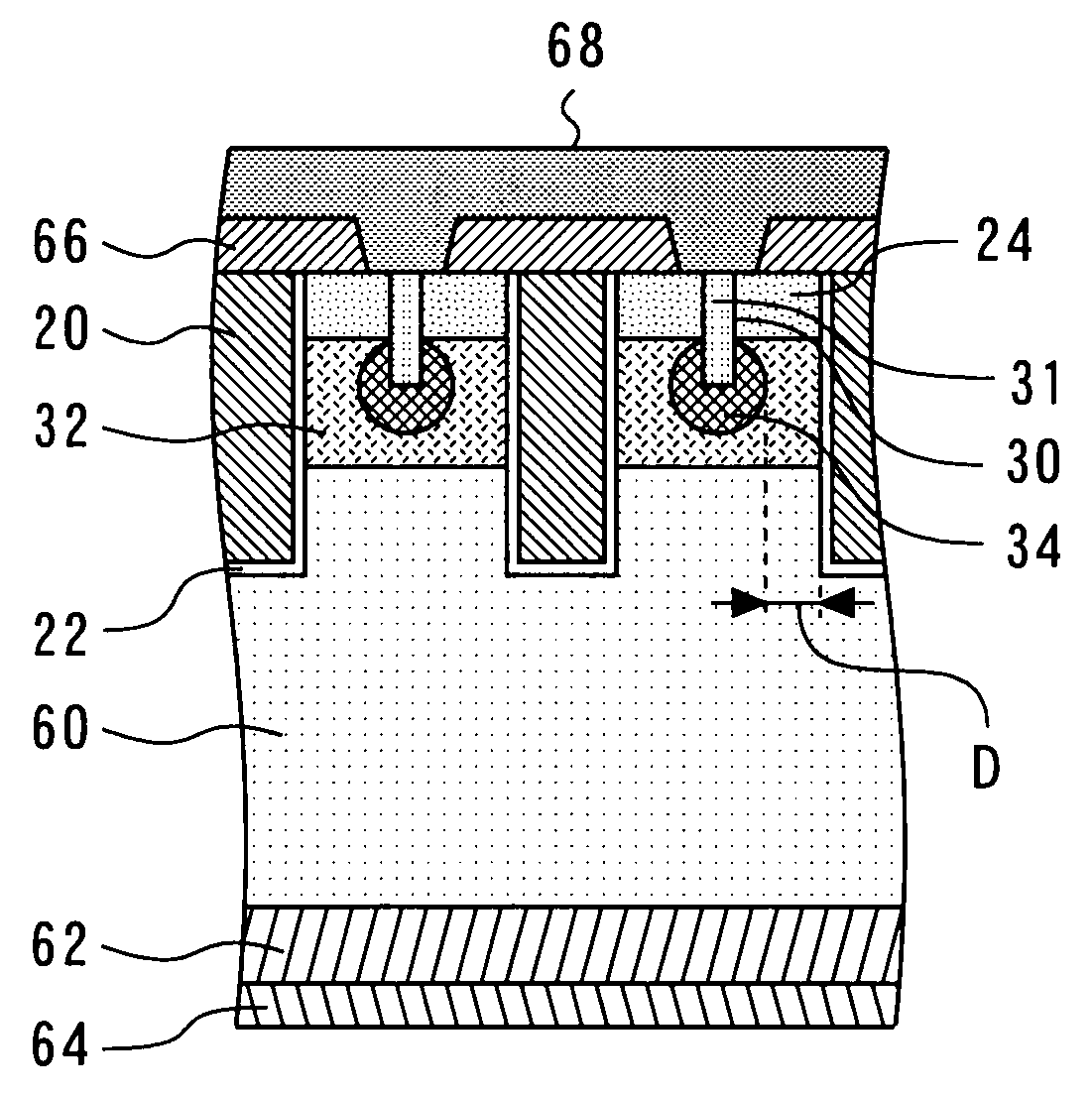
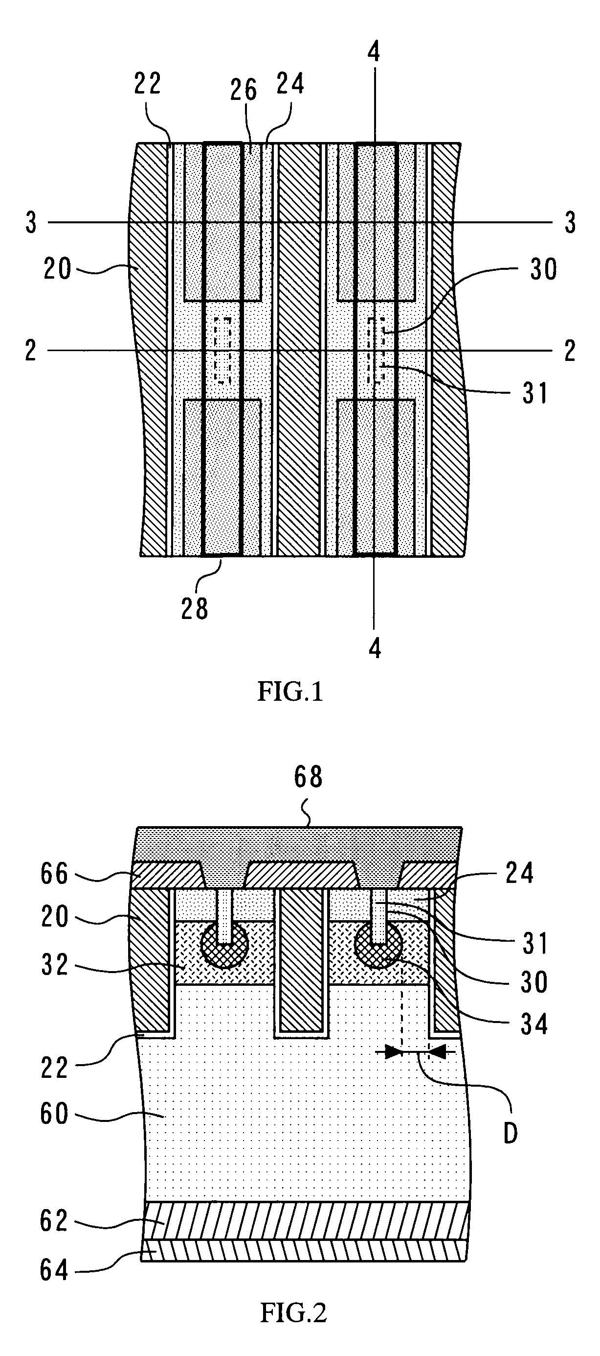
[0030]A first embodiment of the present invention relates to a semiconductor device that is capable of providing latch-up suppression while reducing the influence upon the characteristics of the semiconductor device. FIGS. 1 to 5 are diagrams illustrating the semiconductor device according to the first embodiment. Elements that are shown in these figures and designated by the same reference numerals may not be redundantly described because they are based on the same concept or made of the same materials. This is also true of the drawings illustrating the other embodiments.

[0031]FIG. 1 is a plan view of the semiconductor device according to the present embodiment. A trench gate 20 to which a gate drive signal is transmitted is formed in contact with a gate insulation film 22. A source region 24 is formed in contact with the gate insulation film 22. The source region 24 is a region where an n-type impurity is doped. Further, a P+ region 26 is formed in contact with the source region 2...

second embodiment

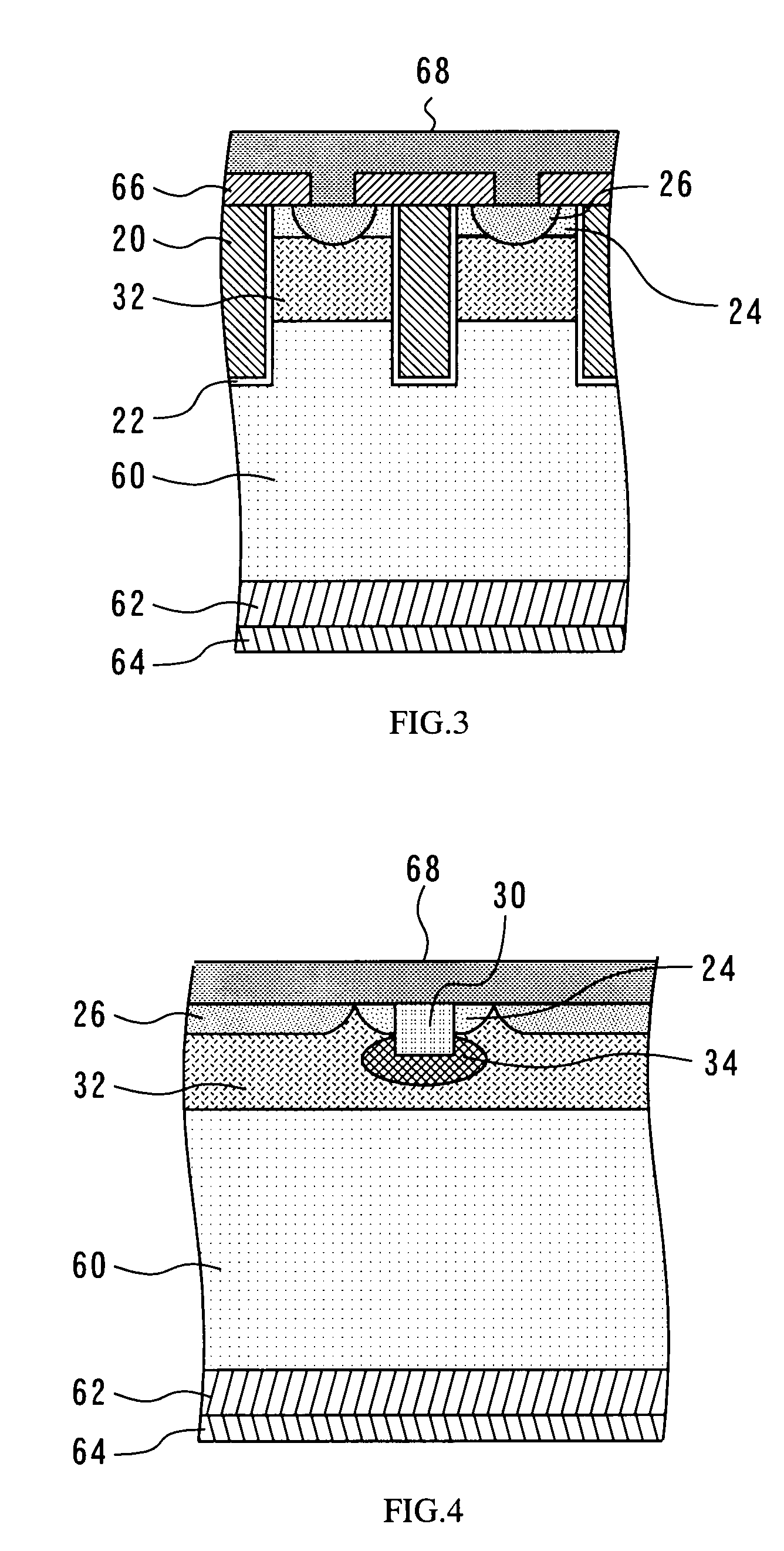
[0060]A second embodiment of the present invention relates to a semiconductor device that decreases the resistance of a base region by forming a break in a dummy trench. The second embodiment will now be described with reference to FIGS. 6 to 17.

[0061]FIG. 6 is a plan view of the semiconductor device according to the present embodiment. FIG. 6 indicates that a dummy trench 23 is formed linearly and discontinuously with a break. The dummy trench 23 is usually formed in parallel with the trench gate 20. The source region 24 is formed along the gate insulation film 22. The source region 24 has a short portion and a long portion, which are formed in the direction from the gate insulation film 22 to the dummy trench 23. The long portion is formed to reach the break in the dummy trench 23.

[0062]FIG. 7 illustrates the break in the dummy trench 23. The dummy trench 23 is a trench gate that is thinned out, and does not receive the supply of a gate drive signal. The dummy trench 23 is formed ...


PUM


Abstract

A semiconductor device includes a substrate of a first conductivity type, a base region of a second conductivity type, a source region of the first conductivity type, a collector region of the second conductivity type, a trench gate, which is formed in a trench via a gate insulation film, an electrically conductive layer, which is formed within a contact trench that is formed through the source region, a source electrode, which is in contact with the electrically conductive layer and the source region, and a latch-up suppression region of the second conductivity type, which is formed within the base region, in contact with the electrically conductive layer, and higher in impurity concentration than the base region. The distance between the gate insulation film and the latch-up suppression region is not less than the maximum width of a depletion layer that is formed in the base layer by the trench gate.

Description

BACKGROUND OF THE INVENTION[0001]1. Field of the Invention[0002]The present invention relates to a semiconductor device that suppresses latch-up by decreasing the resistance of a base region.[0003]2. Background Art[0004]Semiconductor devices called “power devices,” such as IGBTs (Insulated Gate Bipolar Transistors), have been improved to handle high voltages and large currents and widely used with power control apparatuses for use, for instance, in bullet trains and in the fields of transportation and industrial equipment.[0005]The above semiconductor devices control a large current by performing switching operations such as turn-on and turn-off. It is desired that a switching operation be performed in a region called a safe operating area (SOA). The SOA is defined as a safety operating area where a semiconductor device turns on and turns off. More specifically, the SOA defines a range within which the operating locus of a collector current (Ic) and collector-emitter voltage (Vce) i...

Claims


Application Information

Patent Timeline
Patent Type & Authority Patents(United States)
IPC IPC(8): H01L29/76H01L31/119H01L31/113H01L31/062H01L29/94H01L21/336H01L29/739H01L29/78
CPCH01L29/0696H01L29/7397H01L29/41708H01L29/1004
Inventor OKUNO, TAKAHIROKUSUNOKI, SHIGERU
Owner MITSUBISHI ELECTRIC CORP
Why Eureka
Try Eureka