

Semiconductor device and its production method
A manufacturing method and semiconductor technology, applied in the direction of semiconductor/solid-state device manufacturing, semiconductor devices, electric solid-state devices, etc., can solve the problem of increasing the size of semiconductor devices
- Summary
- Abstract
- Description
- Claims
- Application Information
AI Technical Summary
Problems solved by technology
Method used
Image

Examples
no. 1 example )
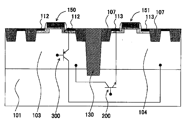
[0057] will refer to Figures 1 to 5 A semiconductor device according to a first embodiment of the present invention is described. figure 1 is a cross-sectional view of the semiconductor device according to the present embodiment. figure 2 is a circuit diagram for describing a diode of the semiconductor device according to the present embodiment. Figures 3 to 5 is a view showing a manufacturing process of the semiconductor device according to the present embodiment.
[0058] Such as figure 1 As shown, the semiconductor device according to this embodiment includes a P-type semiconductor substrate 1, a P-type well region 4 formed on a part of the P-type semiconductor substrate 1, and a P-type well region 4 formed on another part of the P-type semiconductor substrate 1. And the N-type epitaxial layer 2 arranged adjacent to the P-type well region 4 and the N-type buried layer 6 formed under the N-type epitaxial layer 2 .
[0059] P-type semiconductor substrate 1 has, for e...
no. 2 example )
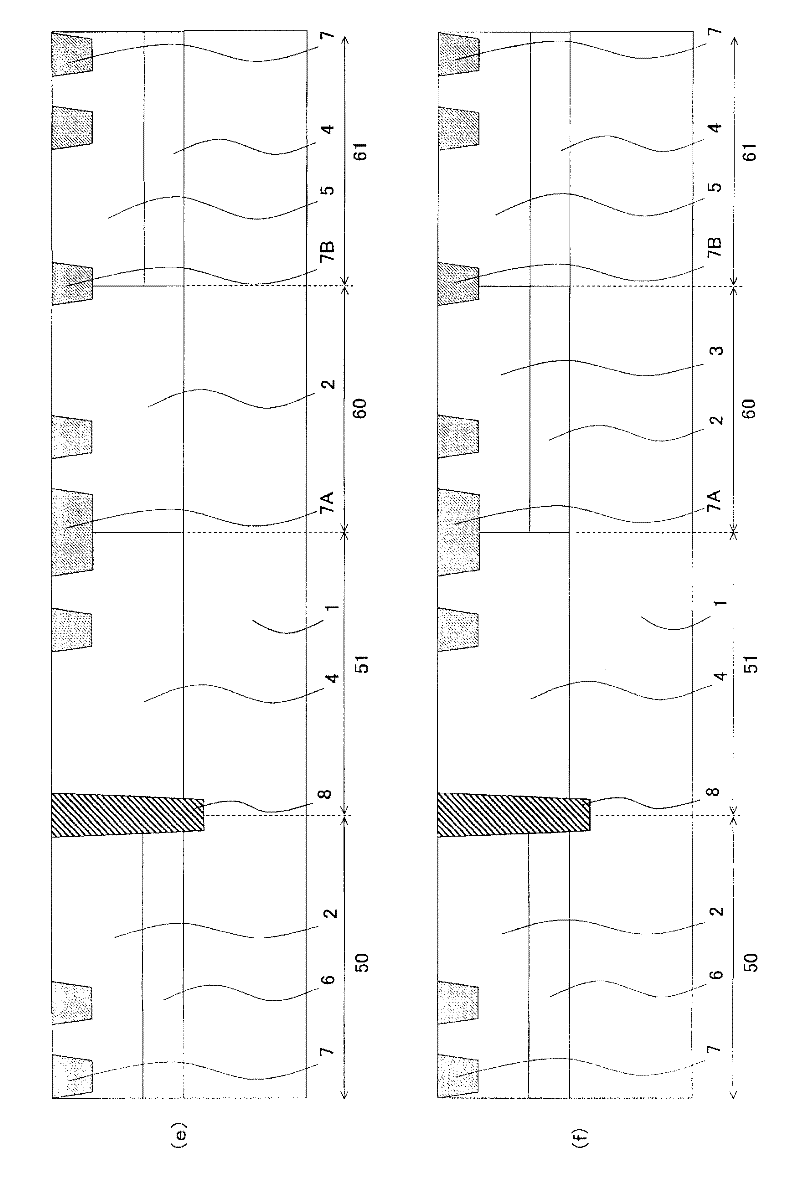
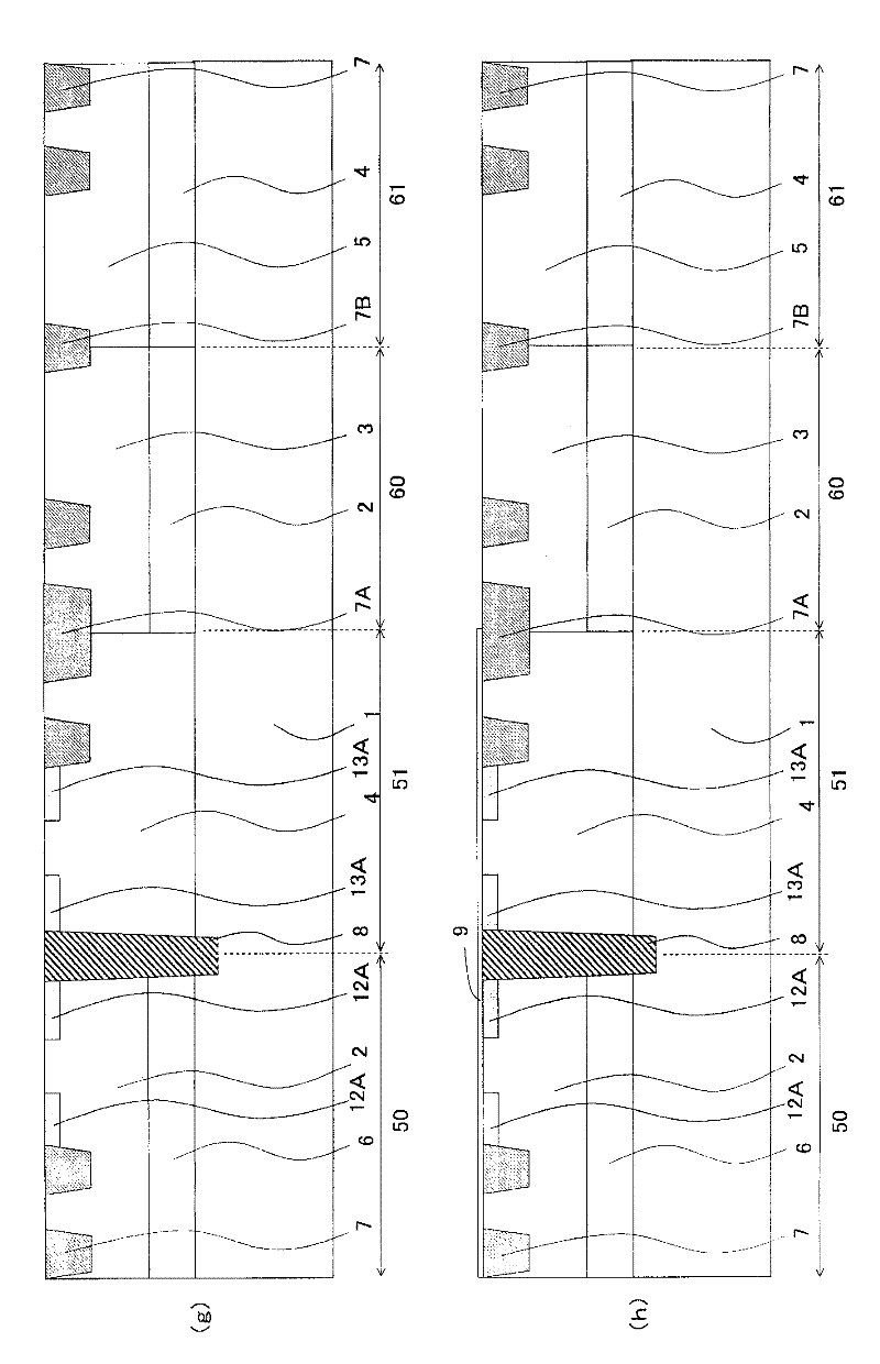
[0098] will now refer to Figures 6 to 12 A semiconductor device according to a second embodiment of the present invention is described. Figure 6 is a cross-sectional view of the semiconductor device according to the second embodiment. Figures 7 to 12 is a view showing a manufacturing process of the semiconductor device according to the second embodiment.
[0099] Such as Figure 6 As shown, the semiconductor device according to the second embodiment is similar to the semiconductor device in the first embodiment, which includes a P-type semiconductor substrate 1, a P-type well region 4, an N-type epitaxial layer 2, an N-type buried layer 6, and a deep The trench 8 also includes a PMOS transistor formed on the N-type epitaxial layer 2 and an NMOS transistor formed on the P-type well 14 . The semiconductor device according to the second embodiment further includes an N-type well region 3 and a second P-type well region 5 via a shallow trench 7A, wherein a PMOS low breakdown...
no. 1 example 1
[0112] As in the first embodiment, first prepare to have 1×10 17 / cm 3 P-type semiconductor substrate 1 with an impurity concentration of .
[0113] Then, if Figure 7 As shown in (a), grow on P-type semiconductor substrate 1 with 4×10 16 / cm 3 N-type epitaxial layer 2 with impurity concentration and thickness of 3 μm. The process is the same as that described in the first example image 3 The process in (a) is the same.
[0114] Then, if Figure 7 As shown in (b), a shallow trench 7 is formed on the N-type epitaxial layer 2 by a known process, and a deep trench 8 is formed on the N-type epitaxial layer 2 and the P-type semiconductor substrate 1 . This process is also the same as that in the first embodiment. However, in the second embodiment, shallow trench 7A is formed at the boundary between high breakdown voltage transistor regions 50 and 51 and a region where low breakdown voltage transistors are formed (hereinafter referred to as low breakdown voltage transistor ...
PUM
 Abstract
Description
Claims
Application Information