Radio frequency (RF) laterally diffused metal oxide semiconductor (LDMOS) component and manufacture method

A manufacturing method and device technology, applied in the direction of semiconductor/solid-state device manufacturing, semiconductor devices, electrical components, etc., can solve problems such as large on-resistance, achieve high breakdown voltage, increase impurity concentration, and improve the effect of conduction.

Active Publication Date: 2013-04-10
SHANGHAI HUAHONG GRACE SEMICON MFG CORP
View PDF6 Cites 7 Cited by
  • Summary
  • Abstract
  • Description
  • Claims
  • Application Information

AI Technical Summary

Problems solved by technology

[0015] The structure of this RF LDMOS device generally uses one-step doping to realize the N-type lightly doped region 12 at the drain end. Since the doping concentration of the N-type lightly doped drift region 12 at the drain end is relatively low, it has a large impact While passing through the voltage BV, it also has a large on-resistance Rdson, and the two are mutually restricted

Method used


Image

  • Radio frequency (RF) laterally diffused metal oxide semiconductor (LDMOS) component and manufacture method
  • Radio frequency (RF) laterally diffused metal oxide semiconductor (LDMOS) component and manufacture method
  • Radio frequency (RF) laterally diffused metal oxide semiconductor (LDMOS) component and manufacture method

Examples


Embodiment 1

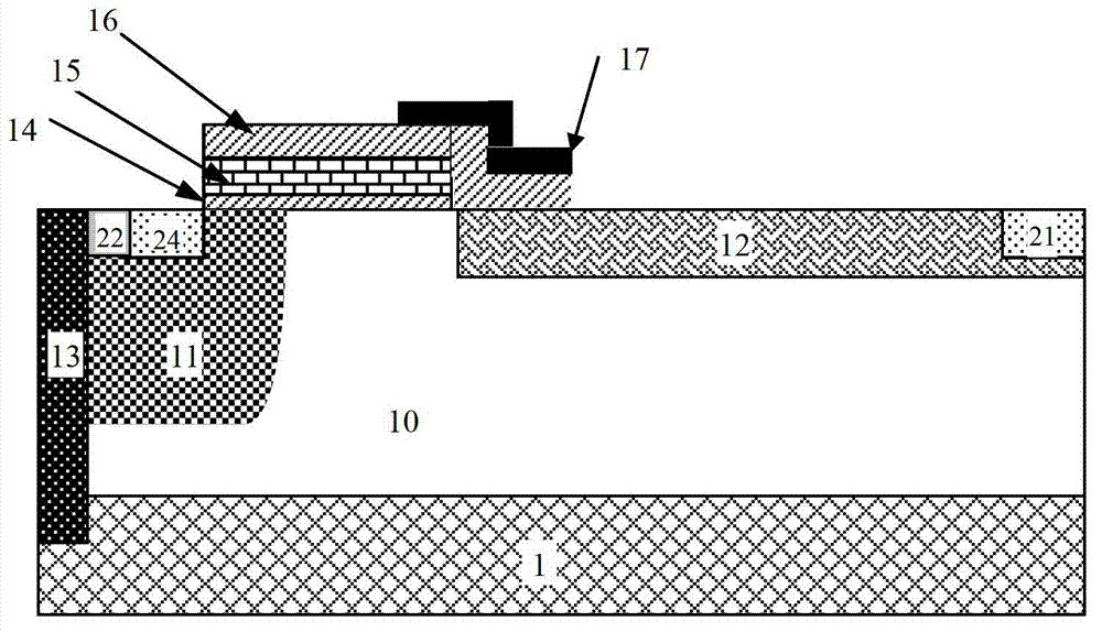
[0067] The structure of RF LDMOS device is as figure 2 shown.

[0068] A P epitaxy 10 is formed on the P substrate 1;

[0069] A P well 11 is formed on the left part of the P epitaxy 10, and a drain N-type lightly doped region 12 is formed on the right part, and the P well 11 is not in contact with the drain N-type lightly doped region 12;

[0070] A source terminal N-type heavily doped region 24 is formed on the upper part of the P well 11;

[0071] A drain N-type heavily doped region 21 is formed on the right of the drain N-type lightly doped region 12;

[0072] An N-type moderately doped region 23 is formed on the left part of the N-type lightly doped region 12 at the drain end;

[0073] The N-type heavily doped region 21 at the drain end is not in contact with the N-type moderately doped region 23;

[0074] The N-type impurity concentration of the N-type medium doped region 23 is less than the N-type impurity concentration of the N-type heavily doped region 21 at the ...

Embodiment 2

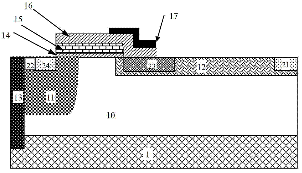
[0083] Such as image 3 As shown, the difference between Embodiment 2 and Embodiment 1 is that a source N-type lightly doped region 18 is formed in the lower edge and right edge of the P well 11 of the source N-type heavily doped region 24, and the source The N-type impurity concentration of the terminal N-type lightly doped region 18 is less than the N-type impurity concentration of the N-type middle-doped region 23; preferably, the N-type impurity is phosphorus or arsenic, and the N-type impurity of the N-type middle-doped region 23 is The range of N-type impurity concentration is 5E17-1E18 cm atoms per cubic centimeter, and the N-type impurity concentration range of source N-type lightly doped region 18 is 1E15-5E17 atoms per cubic centimeter.

Embodiment 3

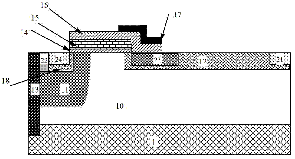
[0085] The manufacturing method of the RF LDMOS device described in embodiment two, comprises the following steps:

[0086] 1. Growing P epitaxy 10 on P substrate 1;

[0087] 2. Forming the P well 11 in the P epitaxy 10 by P ion implantation and high-temperature well pushing (ion activation);

[0088] Preferably, the impurity of the P ion implantation of the P well 11 is boron, the implantation energy range is 30-80KeV, and the implantation dose is 1E 12 ~1E 14 Atoms per square centimeter, the temperature range of high-temperature push well is 800~1200℃, and the time is 10~200 minutes;

[0089] three. growing gate oxide 14 on P epitaxy 10;

[0090] 4. Depositing polysilicon 15 on the gate oxide 14;

[0091] 5. Define the position and area of ​​the polysilicon gate by photoresist 105, the left end of the polysilicon gate is above the right part of the P well 11, and the gate oxide 14 and polysilicon 15 outside the polysilicon gate area are etched away;

[0092] 6. Retain ...


PUM


Abstract

The invention discloses a radio frequency (RF) laterally diffused metal oxide semiconductor (LDMOS) component. A structure of the RF LDMOS component is that a P trap is formed on the left of a P epitaxy, a drain terminal N type light dope region is formed on the right of the P epitaxy, a drain terminal N type heavy dope region is formed on the right of the drain terminal N type light dope region, an N type middle dope region is formed on the left of the drain terminal N type light dope region, and the drain terminal N type heavy dope region is not contacted with the N type middle dope region. The drain terminal N type light dope region of the RF LDMOS component is horizontally and unevenly N doped, the doping concentration of one side close to a polycrystalline silicon gate is high, the doping concentration close to the portion of a drain terminal is low, the component has high breakdown voltage, and simultaneously on resistance of the component is effectively reduced. The invention further discloses a manufacture method of the RF LDMOS component.

Description

technical field [0001] The invention relates to semiconductor technology, in particular to an RF LDMOS device and a manufacturing method thereof. Background technique [0002] RF LDMOS (Radio Frequency Laterally Diffused Metal Oxide Semiconductor) device is a new generation of integrated solid microwave power semiconductor product that is a fusion of semiconductor integrated circuit technology and microwave electronic technology. It has good linearity, high gain, high withstand voltage, and output power. Large size, good thermal stability, high efficiency, good broadband matching performance, easy to integrate with MOS process, etc., and its price is much lower than that of gallium arsenide devices. It is a very competitive power device and is widely used in GSM , PCS, W-CDMA base station power amplifier, and wireless broadcasting and nuclear magnetic resonance, etc. [0003] The breakdown voltage BV and on-resistance Rdson of RF LDMOS devices are two important parameters u...

Claims


Application Information

Patent Timeline
Patent Type & Authority Applications(China)
IPC IPC(8): H01L29/36H01L29/78H01L21/336
Inventor 李娟娟慈朋亮钱文生韩峰董金珠
Owner SHANGHAI HUAHONG GRACE SEMICON MFG CORP
Why Eureka
Try Eureka