LDMOS transistor

Inactive Publication Date: 2006-07-06
DONGBU ELECTRONICS CO LTD
View PDF7 Cites 8 Cited by
  • Summary
  • Abstract
  • Description
  • Claims
  • Application Information

AI Technical Summary

Benefits of technology

[0009] The present invention provides a lateral double-diffused metal oxide semiconductor (LDMOS) transistor, which increases the

Problems solved by technology

There is, however, a trade-off between the on-resistance charact

Method used


Image

  • LDMOS transistor
  • LDMOS transistor

Examples


Example

[0016] Reference will now be made in detail to exemplary embodiments of the present invention, examples of which are illustrated in the accompanying drawings. Wherever possible, like reference designations will be used throughout the drawings to refer to the same or similar parts.

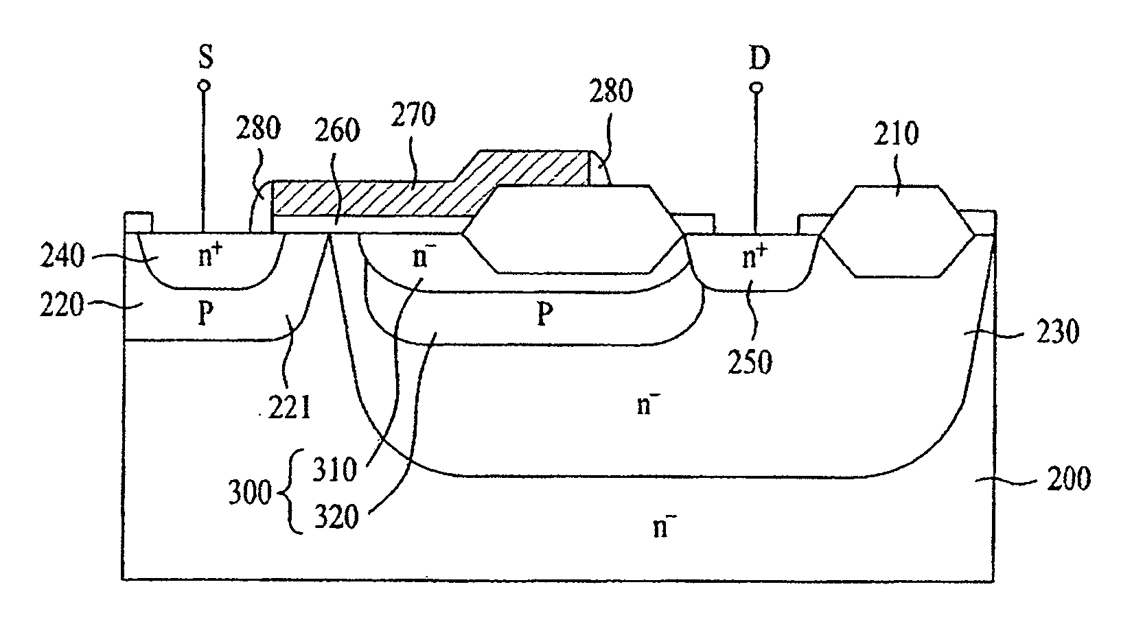
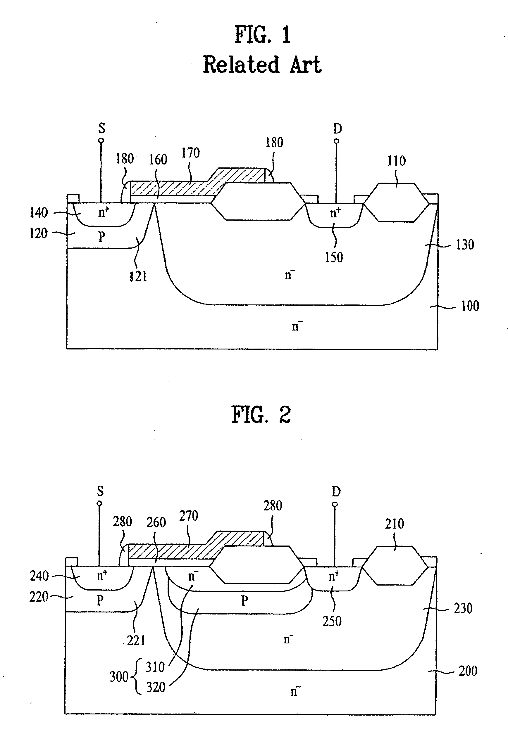
[0017] Referring to FIG. 2, illustrating an exemplary LDMOS transistor according to the present invention, a p-type body 220 and an n− extended drain region 230 spaced apart from one another on an n− semiconductor substrate 200 having an active area defined by a device isolation layer 210. An n+ source region 240 is provided on the p-type body 220. An upper part of the p-type body region 220, which is overlapped by a gate insulating layer 260 and a gate conductive layer 270 near the n+ source region 240, is a channel 221. An n+ drain region 250 is provided on the n− extended drain region 230.

[0018] A depletion region 300 is provided on the n− extended drain region 230 between the p-type body 220 and the n...


PUM


Abstract

A lateral double-diffused metal oxide semiconductor transistor (LDMOS) transistor includes a semiconductor substrate of a first conductivity; an extended drain region of the first conductivity formed in a surface region of the semiconductor substrate; and a depletion region, formed in the extended drain region, including first and second impurity regions sequentially embedded below a surface of the extended drain region, the first embedded impurity region being of a second conductivity and the second embedded impurity region being of the first conductivity.

Description

CROSS-REFERENCE TO RELATED APPLICATION [0001] This application claims the benefit of Korean Patent Application No. 10-2004-0117437, filed on Dec. 30, 2004, which is hereby incorporated by reference as if fully set forth herein. BACKGROUND OF THE INVENTION [0002] 1. Field of the Invention [0003] The present invention relates to a semiconductor device, and more particularly, to a lateral double-diffused metal oxide semiconductor (LDMOS) transistor. Although the present invention is suitable for a wide scope of applications, it is particularly suitable for high breakdown voltage and enhanced on-resistance characteristics. [0004] 2. Discussion of the Related Art [0005] Referring to FIG. 1, illustrating an LDMOS transistor according to the related art, a p-type body 120 and an n− extended drain region 130 are spaced apart from one another on an n− semiconductor substrate 100 having an active area defined by a device isolation layer 110. An n+ source region 140 is provided on the p-type b...

Claims


Application Information

Patent Timeline
IPC IPC(8): H01L29/76
CPCH01L29/0634H01L29/0873H01L29/42368H01L29/66689H01L29/7816H01L21/18
Inventor LEE, SUK KYUN
Owner DONGBU ELECTRONICS CO LTD
Why Eureka
Try Eureka