LED chip and manufacturing method thereof

A technology of light-emitting diodes and manufacturing methods, which is applied in the field of lighting, can solve problems such as reducing the area of ​​light-emitting diodes, achieve uniform current distribution, improve luminous efficiency, and increase the effect of light-emitting area

Active Publication Date: 2010-11-17
JADE BIRD DISPLAY SHANGHAI LTD
View PDF5 Cites 9 Cited by
  • Summary
  • Abstract
  • Description
  • Claims
  • Application Information

AI Technical Summary

Problems solved by technology

[0005] The invention provides a light-emitting diode and its manufacturing method to solve the problem that the area of ​​the light-emitting diode is reduced by the manufacturing method of p and n electrodes in the prior art

Method used


Image

  • LED chip and manufacturing method thereof
  • LED chip and manufacturing method thereof
  • LED chip and manufacturing method thereof

Examples


Embodiment approach

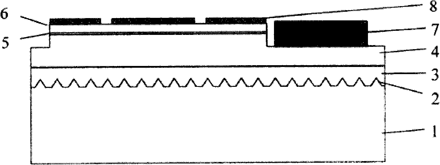
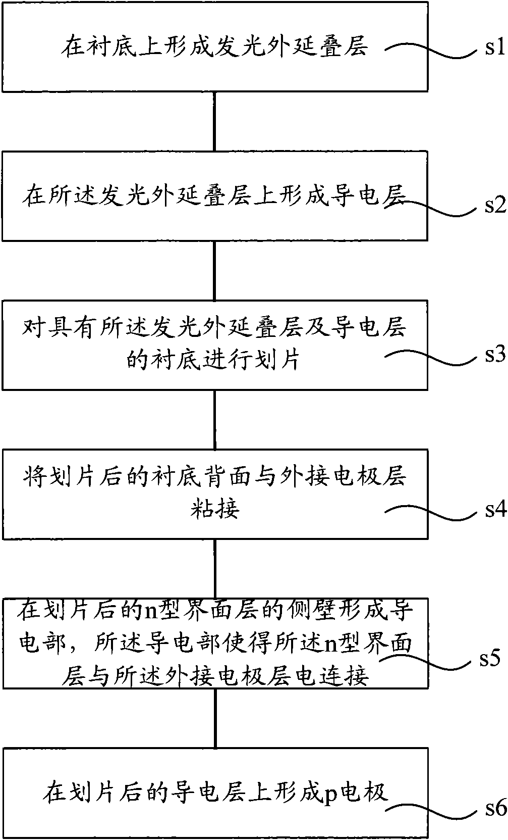
[0024] refer to figure 2 As shown, an embodiment of the light-emitting diode chip manufacturing method of the present invention includes:

[0025] Step s1, forming a light-emitting epitaxial stack on the substrate, which sequentially includes: forming an n-type interface layer on the substrate; forming a light-emitting layer on the n-type interface layer; forming a p-type interface layer on the light-emitting layer;

[0026] Step s2, forming a conductive layer on the light-emitting epitaxial stack;

[0027] Step s3, dicing the substrate having the light-emitting epitaxial stack and the conductive layer;

[0028] Step s4, bonding the back of the diced substrate to the external electrode layer;

[0029] Step s5, forming a conductive portion on the sidewall of the n-type interface layer after scribing, and the conductive portion electrically connects the n-type interface layer to the external electrode layer;

[0030] Step s6, forming a p-electrode on the diced conductive lay...


PUM


Abstract

The invention relates to an LED chip and a manufacturing method thereof. The LED chip comprises a substrate and a luminous epitaxial stack on the substrate, wherein the luminous epitaxial stack sequentially comprises an n-shaped interface layer, a luminous layer on the n-shaped interface layer and a p-shaped interface layer on the luminous layer. The area of the p-shaped interface layer is same as that of the luminous layer and the n-shaped interface layer; the p-shaped interface layer is provided with a p electrode; the back surface of the substrate is provided with an external electrode layer; and the side wall of the n-shaped interface layer is electrically connected with the external electrode layer by a conductive part.

Description

technical field [0001] The invention relates to lighting technology, in particular to a light-emitting diode chip and a manufacturing method thereof. Background technique [0002] A light emitting diode (LED, Light Emitting Diode) is a solid-state semiconductor device that can convert electrical energy into visible light. Due to its advantages of small size, low power consumption and long service life, it has gradually replaced traditional light sources and is more and more widely used in the lighting field. [0003] At present, III-V nitride semiconductor materials have been widely used in the manufacturing process of light-emitting diodes. Taking GaN as an example, it is usually grown on a sapphire substrate. However, since sapphire itself is an insulator, its conductive properties cannot be changed by means such as doping. Therefore, it is necessary to electrically connect the light emitting diode device grown on the sapphire substrate with the outside through electrod...

Claims


Application Information

Patent Timeline
Patent Type & Authority Applications(China)
IPC IPC(8): H01L33/36H01L33/14
Inventor 张汝京
Owner JADE BIRD DISPLAY SHANGHAI LTD
Why Eureka
Try Eureka