Power supply switching circuit

a switching circuit and power supply technology, applied in the direction of power conversion systems, logic circuit coupling arrangements, pulse techniques, etc., can solve problems such as power loss

Inactive Publication Date: 2010-09-21
ABLIC INC
View PDF9 Cites 17 Cited by
  • Summary
  • Abstract
  • Description
  • Claims
  • Application Information

AI Technical Summary

Benefits of technology

[0009]The present invention has been made in view of the above-mentioned problem, and it is an object thereof to provide a power supply switching circuit capable of effectively supplying a desired voltage among a plurality of voltages to a load.
[0012]Therefore, the power supply switching circuit of the present invention can supply the load effectively with a desired voltage among a plurality of voltages.

Problems solved by technology

However, the above-mentioned circuit may cause a power loss because the voltage supplied from the battery to the load is dropped by a forward voltage drop of the rectifier diode.
However, the conventional power supply switching circuit illustrated in FIG. 4 has a problem that if a semiconductor substrate is of P type, a higher voltage between a voltage of the AC adapter 23 and a voltage of the battery 20 may be supplied to the load 28 because of a parasitic diode existing in the P-type MOS transistor.

Method used


Image

  • Power supply switching circuit
  • Power supply switching circuit
  • Power supply switching circuit

Examples


first embodiment

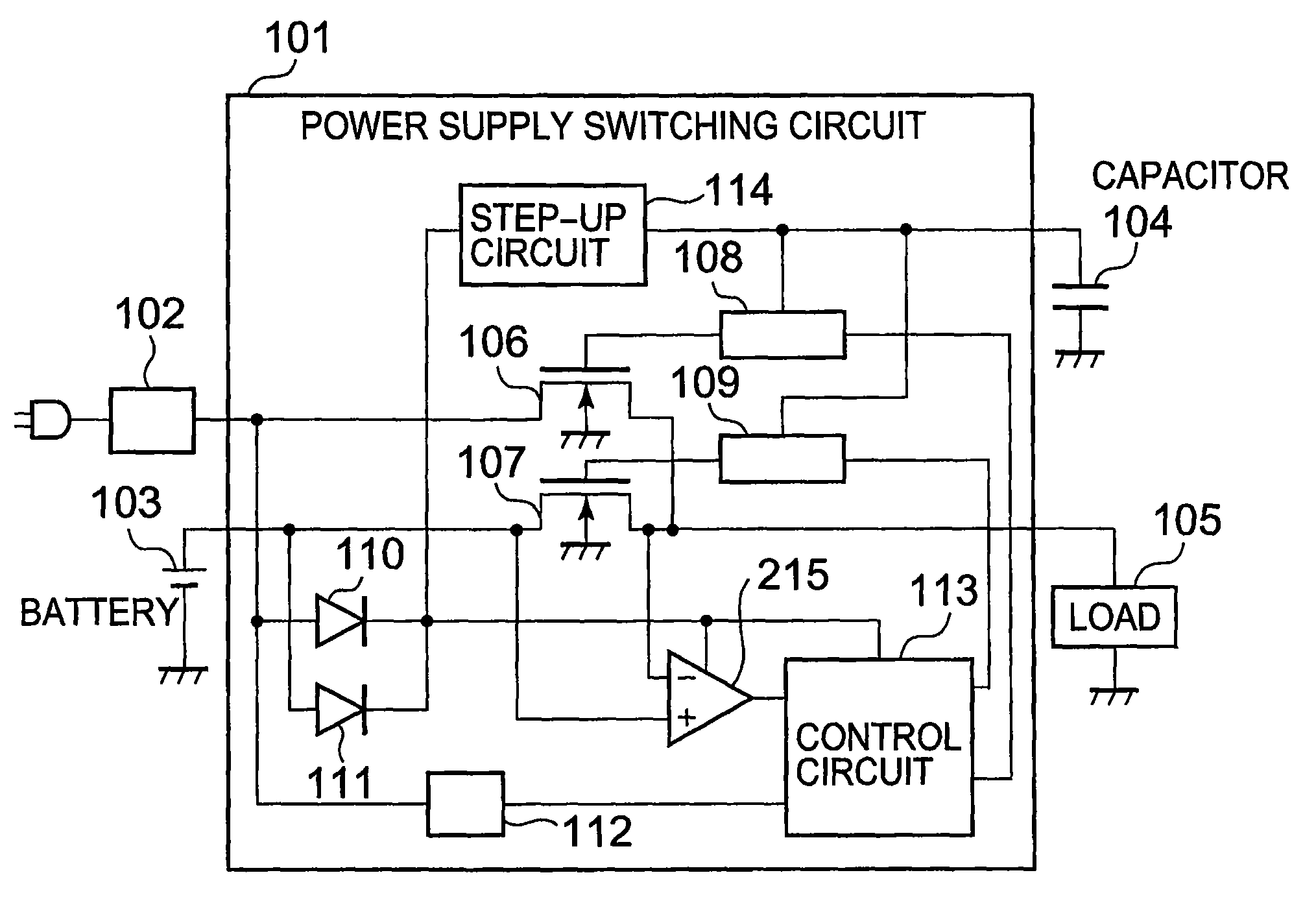
[0019]In the first place, a structure of a power supply switching circuit according to a first embodiment of the present invention is described. FIG. 1 is a diagram illustrating the power supply switching circuit of the first embodiment of the present invention.

[0020]Here, a power supply switching circuit 101 is formed on a semiconductor substrate of P type as a first conductive type.

[0021]The power supply switching circuit 101 includes N-type MOS transistors 106 and 107, level shifters 108 and 109, diodes 110 and 111, an AC adapter detection circuit 112, a control circuit 113, and a step-up circuit 114. The power supply switching circuit 101 is connected to an AC adapter 102, a battery 103, a capacitor 104, and a load 105, for example, as a peripheral circuit.

[0022]A first power source terminal for connecting to the AC adapter 102 is connected to a drain of the N-type MOS transistor 106, an anode of the diode 110 and an input terminal of the AC adapter detection circuit 112. A seco...

second embodiment

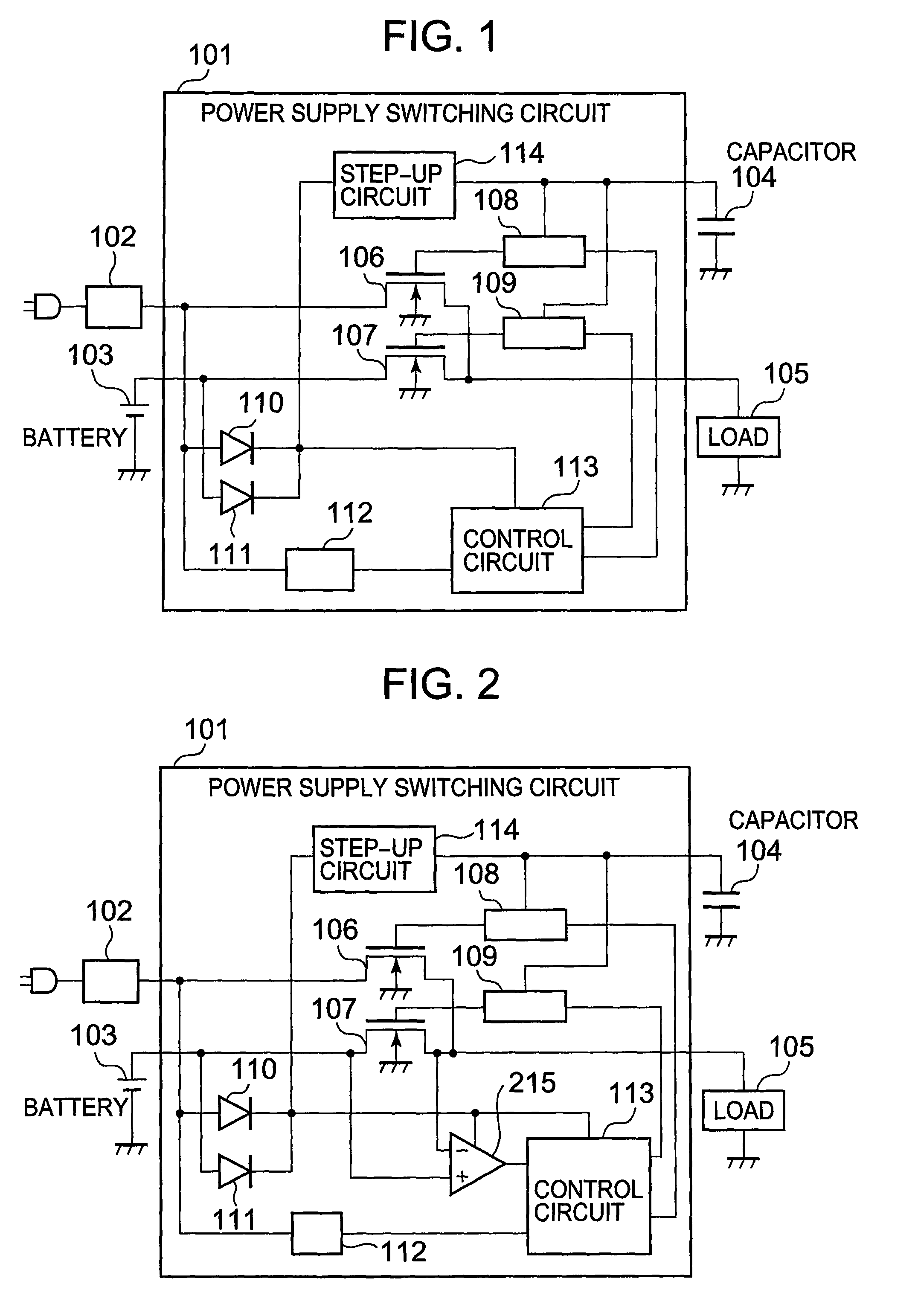
[0038]Next, a power supply switching circuit 101 according to a second embodiment of the present invention is described. Here, as a condition of a peripheral device, it is supposed that the load 105 includes a capacitor (not shown) for stabilizing power supply, and that the voltage of the AC adapter 102 is higher than the voltage of the battery 103.

[0039]FIG. 2 is a diagram illustrating the power supply switching circuit of the second embodiment. The power supply switching circuit of the second embodiment includes a comparator 215 in addition to the power supply switching circuit of the first embodiment.

[0040]A power source terminal of the comparator 215 is connected to the cathodes of the diodes 110 and 111, a noninverting input terminal thereof is connected to the drain of the N-type MOS transistor 107, an inverting input terminal thereof is connected to the source of the N-type MOS transistor 107, and an output terminal thereof is connected to a second input terminal of the contr...

third embodiment

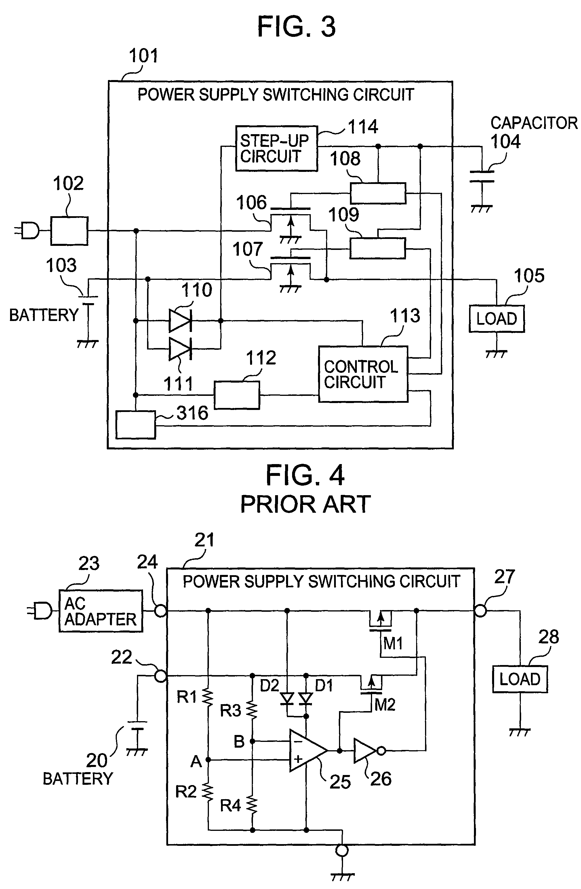
[0045]Next, a structure of a power supply switching circuit 101 according to a third embodiment of the present invention is described. FIG. 3 is a diagram illustrating the power supply switching circuit of the third embodiment.

[0046]The power supply switching circuit of the third embodiment includes a pull-down circuit 316 in addition to the power supply switching circuit of the first embodiment.

[0047]A power source terminal of the pull-down circuit 316 is connected to the first power source terminal to which the AC adapter 102 is connected, and an output terminal thereof is connected to a second input terminal of the control circuit 113.

[0048]Next, an operation of the power supply switching circuit of the third embodiment is described.

[0049]103 is connected to the power supply switching circuit 101>

[0050]The first power source terminal for connecting to the AC adapter 102 is opened, and hence it is easily affected by noise or a leak current. Therefore, a detection error may occur i...


PUM


Abstract

Provided is a power supply switching circuit capable of efficiently supplying a desired voltage among a plurality of voltages to a load. In the case of a P-type semiconductor substrate, N-type MOS transistors are provided between a load and an AC adapter and between the load and a battery, and hence no parasitic diode exists between the load and the AC adapter or the battery, resulting in no current path due to the parasitic diode. Thus, when the AC adapter and the battery are connected to the power supply switching circuit, the N-type MOS transistor is turned off, whereby the current path between the battery and the load is cut off completely and the N-type MOS transistor is turned on. Accordingly, the battery cannot supply a voltage to the load while only the AC adapter can supply a voltage to the load.

Description

RELATED APPLICATIONS[0001]This application claims priority under 35 U.S.C. § 119 to Japanese Patent Application No. JP2007-335808 filed on Dec. 27, 2007, the entire content of which is hereby incorporated by reference.BACKGROUND OF THE INVENTION[0002]1. Field of the Invention[0003]The present invention relates to a power supply switching circuit for switching power supply voltages to be supplied to a load.[0004]2. Description of the Related Art[0005]Portable electronic devices and the like are designed to operate with a plurality of power supplies like an AC adapter and a battery. In general, a voltage of the AC adapter is higher than a voltage of the battery. When the AC adapter is connected to a rechargeable electronic device, a power supply voltage is supplied from the AC adapter to a load. In this case, a rectifier diode disposed between the power supply and the load prevents a current from flowing from the AC adapter to the battery.[0006]However, the above-mentioned circuit may...

Claims


Application Information

Patent Timeline
Patent Type & Authority Patents(United States)
IPC IPC(8): H02M1/10
CPCH03K19/017545H03K17/693H02J9/06H02M1/36
Inventor YOSHIKAWA, KIYOSHIUTSUNOMIYA, FUMIYASUTSUZAKI, TOSHIYUKIMASUKO, HIROYUKIUEHARA, OSAMUWAKE, HIROKIDEGUCHI, MICHIYASU
Owner ABLIC INC
Why Eureka
Try Eureka