Semiconductor device with interconnection structure for reducing stress migration

a technology of interconnection structure and semiconductor, applied in the field of semiconductor devices, can solve problems such as unclear how stress migration can be reduced, and achieve the effect of reducing stress migration

Active Publication Date: 2010-10-05
RENESAS ELECTRONICS CORP
View PDF36 Cites 29 Cited by
  • Summary
  • Abstract
  • Description
  • Claims
  • Application Information

AI Technical Summary

Benefits of technology

[0008]It is an object of the present invention to provide a semiconductor device having an interconnection structure for reducing stress migration and a method of fabricating such a semiconductor device.
[0011]In the present invention, the plug sidewall angle in the cross-sectional shape of the via-plug does not become a negative angle, and as a result, shape that would cause stress to concentrate are not formed in the via-plug sidewalls of the via-plug cross-sectional shape. In addition, because a minimum value exists between the two maximum values for the plug sidewall angle, an inclination of the sidewall changes such that a via-hole diameter increases midway from the via-plug base to the top, and the essential aspect ratio of the via-hole is therefore smaller than for a simple tapered shape.
[0015]In addition, the amenability of the via-hole interiors to filling with metal is further improved when the plug sidewall angle is less than 90° between the via-plug base and the points on via-plug sidewalls at which the plug sidewall angle becomes a minimum value between maximum values.
[0016]Moreover, the amenability of the via-hole interiors to filling with metal is further improved if a metal diffusion barrier film is included on the first interconnection, and if the plug sidewall angle at the position of the side surface of the metal diffusion barrier film is less than 90°.
[0017]Accordingly, shapes that would bring about a concentration of stress are not formed on the via-plug sidewalls in the semiconductor device of the present invention, and as a result, the via-hole interior is more amenable to filling with metal, and the occurrence of voids can be prevented. Moreover, stress migration is reduced and the reliability of the interconnections is improved.

Problems solved by technology

However, although the effect of the shape of via-plugs upon stress migration has been touched upon in the above-described literature, nothing has been disclosed regarding methods of solving this problem, and it is unclear how stress migration can be reduced.

Method used


Image

  • Semiconductor device with interconnection structure for reducing stress migration
  • Semiconductor device with interconnection structure for reducing stress migration
  • Semiconductor device with interconnection structure for reducing stress migration

Examples


first working example

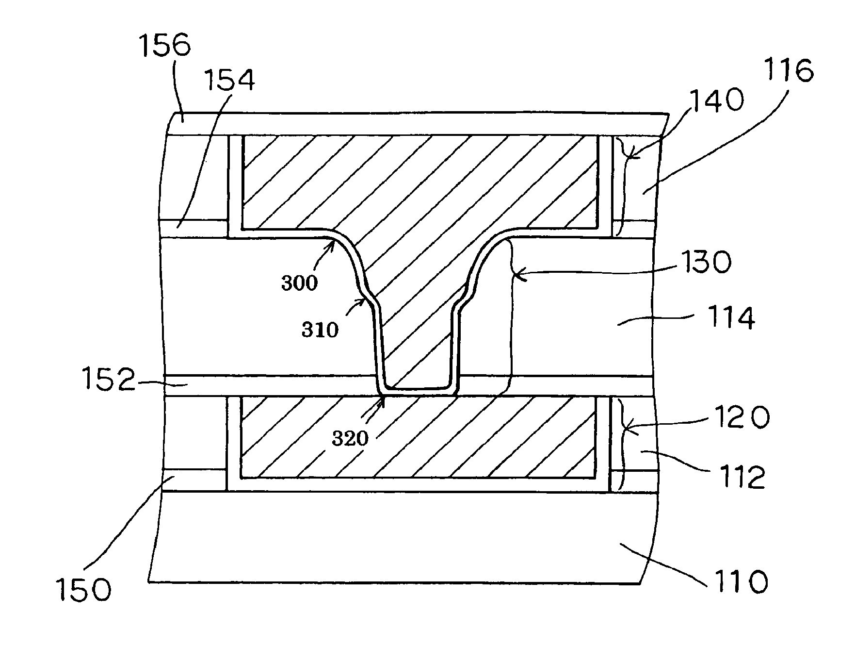
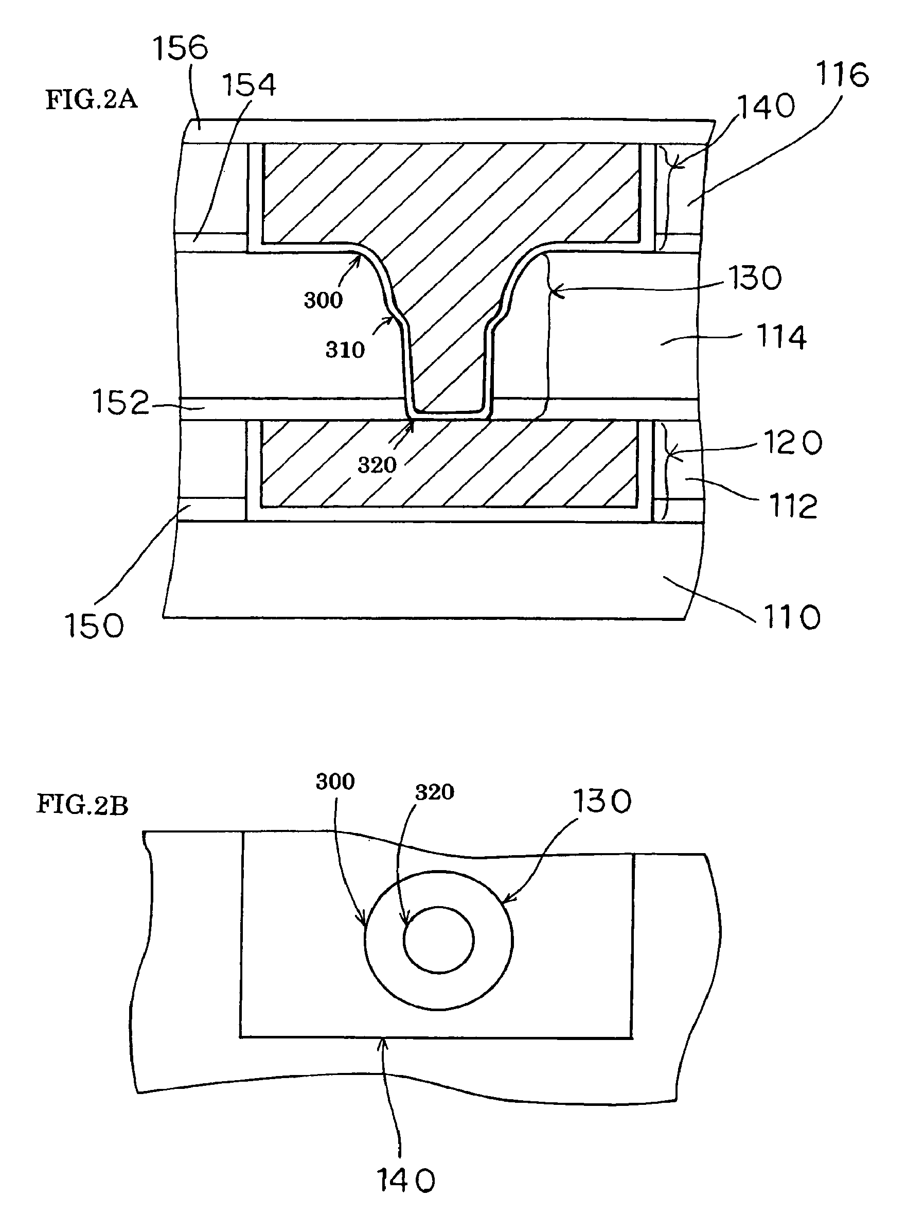
[0029]As shown in FIG. 2A, the semiconductor device is a configuration that includes: interconnection 120 on lower dielectric film 110 that is formed on a semiconductor substrate (not shown); via-plug 130 that is connected to interconnection 120; and interconnection 140 that is connected to via-plug 130. Via-plug 130 and interconnection 140 are formed as a single unit. Interconnection 120, via-plug 130, and interconnection 140 each include the conductive material copper (Cu) and a barrier metal film for preventing diffusion of the copper.

[0030]Intralayer dielectric film 112 for insulating interconnection 120 from interconnections that are formed on the same level is formed on lower dielectric film 110. The upper surface of interconnection 120 is covered by Cap-SiCN film 152, which forms a metal diffusion prevention film for preventing the diffusion of copper at points other than the points of connection with via-plug 130. Interconnection 140 is formed in intralayer dielectric film 1...

second working example

[0072]The present working example is a semiconductor device that is provided with a via-plug in which only a portion of the via-plug has the sidewall shape of the via-plug in the first working example.

[0073]The following explanation regards the semiconductor device of the present working example. Identical reference numerals are applied to components that are identical to those of the first working example and detailed explanation of such components is here omitted. In addition, the fabrication for this working example is identical to that of the first working example and explanation of this method is therefore here omitted.

[0074]As shown in FIG. 8A, the semiconductor device of this working example is a configuration that includes: interconnection 120; via-plug 136 that is connected to interconnection 120; and interconnection 146 that is formed as a single unit with via-plug 136. Regarding the sectional shape of the via-plug sidewall that is shown in FIG. 8A, the left side of the fi...


PUM


Abstract

The semiconductor device of the present invention includes a first interconnection, a via-plug that is connected to the first interconnection, and a second interconnection that is formed as a single unit with the via-plug. The cross-sectional shape of the via-plug is such that the plug sidewall angle, which indicates the angle of the via-plug sidewall with respect to the surface of the first interconnection, is a positive angle; and moreover, at least two points exist between the base and the top of the via-plug on at least one sidewall of the two sidewalls of the cross-sectional shape of the via-plug at which the plug sidewall angle attains a maximum value. Since shapes that would give rise to the occurrence of concentrations of stress are not formed in the via-plug sidewalls, metal is more effectively embedded in the via-hole, and the incidence of voids is prevented.

Description

[0001]This is a divisional of application Ser. No. 10 / 855,562 filed May 28, 2004. The entire disclosure of the prior application, application Ser. No. 10 / 855,562 is hereby incorporated by reference.BACKGROUND OF THE INVENTION[0002]1. Field of the Invention[0003]The present invention relates to a semiconductor device having interconnections and a via-plug for connecting the interconnections together, and to a fabrication method for such a semiconductor device.[0004]2. Description of the Related Art[0005]Among semiconductor devices such as memory and logic devices are those that conventionally include an interconnection structure in which interconnections are connected together by via-plugs. FIG. 1 is a sectional view showing an example of the configuration of a semiconductor device of the prior art. As shown in FIG. 1, the semiconductor device is a configuration that includes: interconnection 120 on lower dielectric film 110 that is formed on a semiconductor substrate (not shown); vi...

Claims


Application Information

Patent Timeline
Patent Type & Authority Patents(United States)
IPC IPC(8): H01L21/4763H01L21/768H01L23/522H01L23/532
CPCH01L21/76804H01L21/76808H01L21/76877H01L23/5226H01L23/53238H01L23/5329H01L23/53295H01L2924/0002H01L2924/00
Inventor KAWANO, MASAYAYAMAMOTO, YOSHIAKIITO, TAKAMASA
Owner RENESAS ELECTRONICS CORP
Why Eureka
Try Eureka