
TSV-enabled twisted pair

a technology of twisted pair and twisted pair, which is applied in the direction of semiconductor devices, semiconductor/solid-state device details, electrical apparatus, etc., can solve the problems of increasing circuit density, significant amount of area to implement, and increasing troubl

Active Publication Date: 2010-10-12
TAIWAN SEMICON MFG CO LTD
View PDF2 Cites 14 Cited by
  • Summary
  • Abstract
  • Description
  • Claims
  • Application Information

AI Technical Summary

Benefits of technology

The patent text describes a system, structure, and method for forming a twisted pair in a semiconductor device using through substrate vias (TSVs). The technical effects of this invention include improved performance and reliability of semiconductor devices, reduced interference between neighboring conductive lines, and improved signal quality. The invention can be applied to a variety of integrated circuit devices, such as microprocessors, memory devices, and sensors.

Problems solved by technology

This problem becomes increasingly troublesome as circuits shrink and the density of the circuits increase.
This method, however, requires a significant amount of area to implement and, thus, may require a larger die to implement a given circuit.
In this attempt, however, the twisted pair has limited tunability in terms of characteristic impedance.
Furthermore, the material in the core of the twists is not easily changed and devices cannot be placed in the core to further influence the characteristics of the signal.
This attempt also requires additional die space and several metal layers due to the 3D geometry.

Method used


Image

  • TSV-enabled twisted pair
  • TSV-enabled twisted pair
  • TSV-enabled twisted pair

Examples


Embodiment Construction

[0017]The making and using of the presently preferred embodiments are discussed in detail below. It should be appreciated, however, that an illustrative embodiment provides many applicable inventive concepts that can be embodied in a wide variety of specific contexts. The specific embodiments discussed are merely illustrative of specific ways to make and use the invention, and do not limit the scope of the invention.

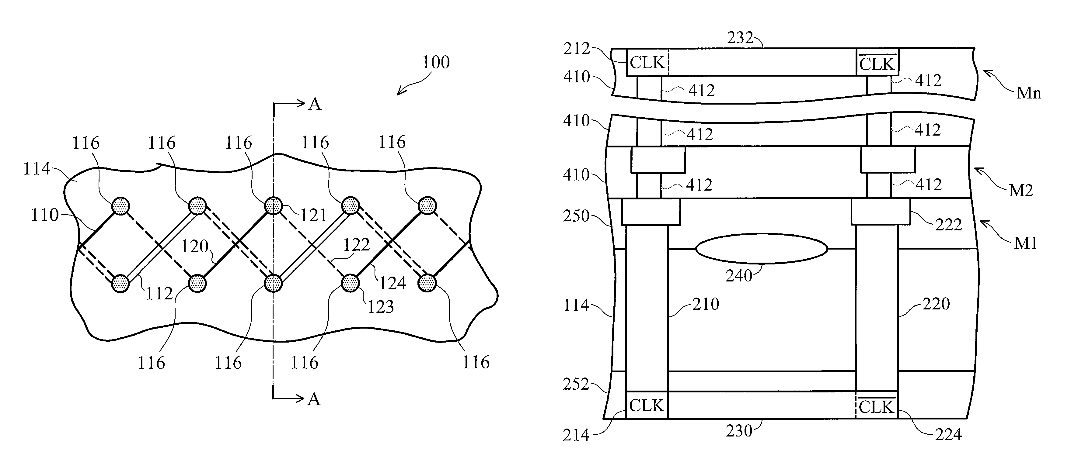
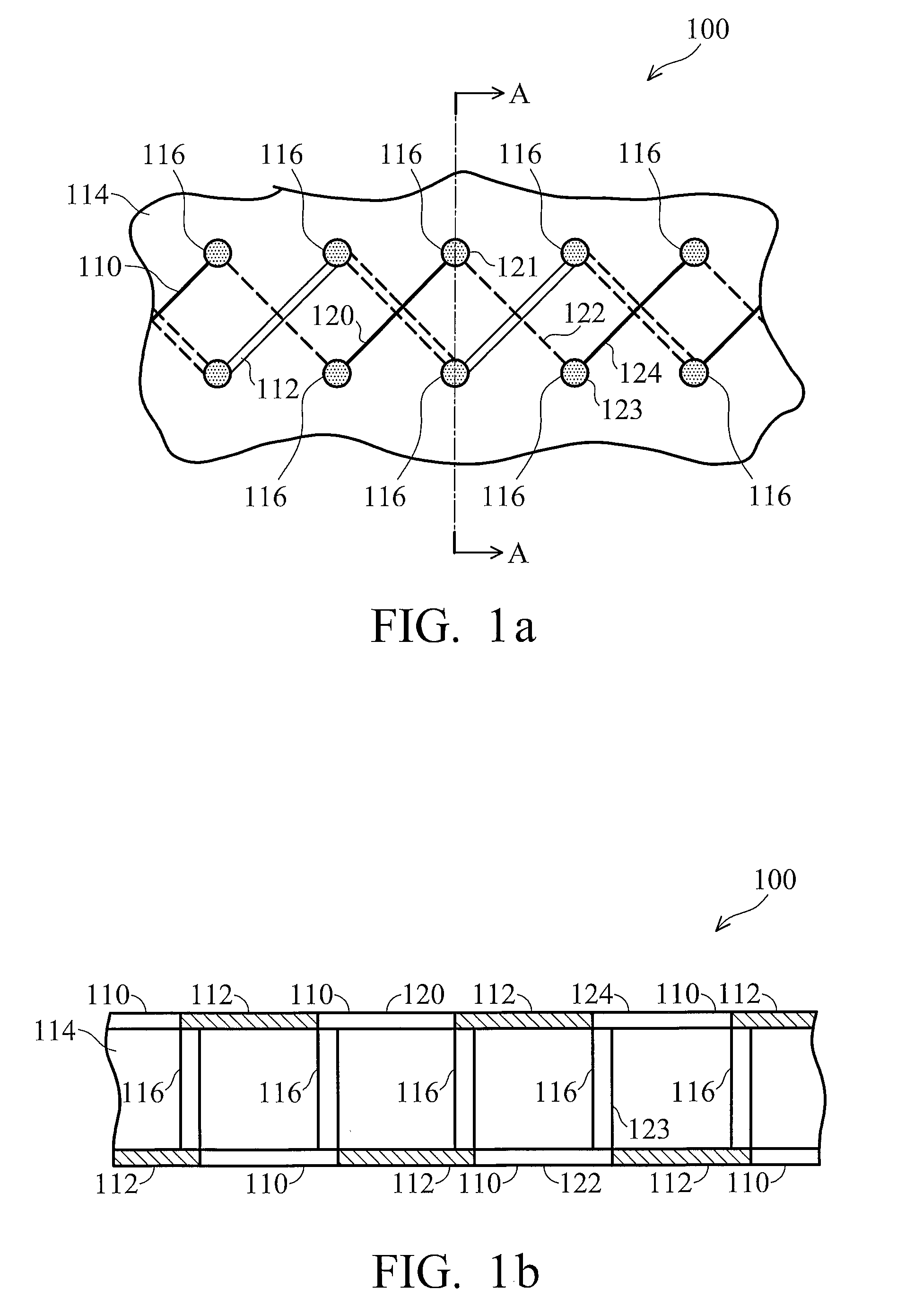
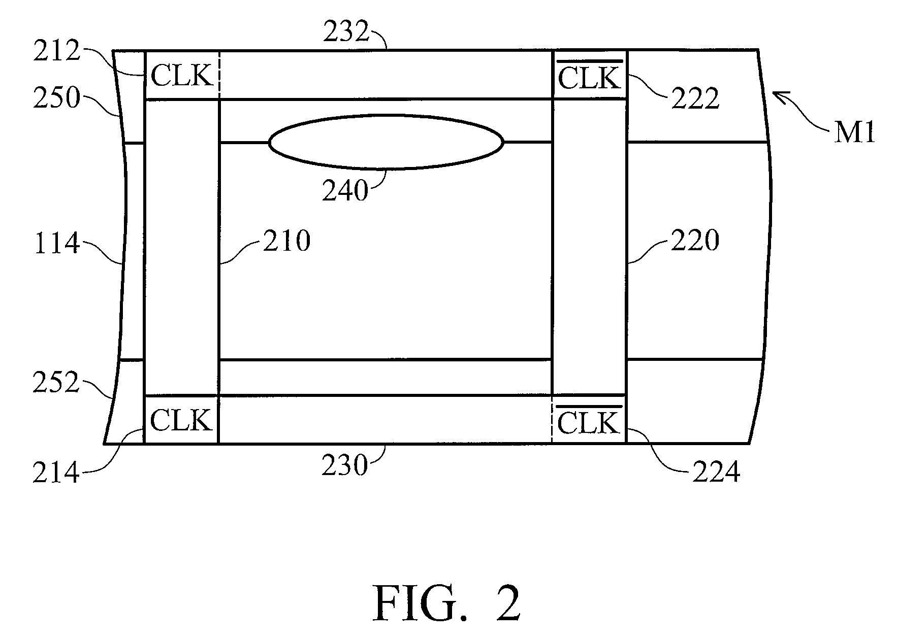
[0018]With reference now to FIGS. 1a and 1b, a top view and a side view, respectively, are shown of a twisted pair 100 in accordance with an embodiment of the present invention. The twisted pair 100 includes a first conductive line 110 and a second conductive line 112 such that each of the first conductive line 110 and the second conductive line 112 include alternating sections of conductive trace on the opposing sides of a substrate 114. For illustrative purposes, the first conductive line 110 is illustrated as a single line and the second conductive line 112 is illustr...


PUM


Abstract

A through-silicon via (TSV) enabled twisted pair is provided. A pair of complementary conductive lines is provided as a twisted pair. Each of the conductive lines of the twisted pair is formed by alternating conductive sections on opposing sides of a substrate. The alternating conductive sections are electrically coupled by at least in part a TSV. The conductive lines overlap or are entwined such the point at which the conductive lines cross, the conductive lines are on opposing sides of the substrate. The conductive lines are weaved in this manner for the length of the conductive trace.

Description

TECHNICAL FIELD[0001]The present invention relates generally to semiconductor devices and, more particularly, to using through substrate vias (TSVs) to form twisted pairs on an integrated circuit.BACKGROUND[0002]Integrated circuits generally comprise electrical traces electrically coupled to electronic devices, such as transistors, capacitors, resistors, and the like. As the size of the integrated circuits decrease, the electrical components, including the electrical traces and the electronic devices, become closer to each other. As is known in the art, a phenomenon referred to as crosstalk may occur wherein a signal transmitted on one line may create an undesired effect on another. This problem becomes increasingly troublesome as circuits shrink and the density of the circuits increase.[0003]One attempt at reducing the effect of crosstalk is to shield the affected traces. In this attempt, critical signals such as clock signals are surrounded or shielded by metal traces and vias tha...

Claims


Application Information

Patent Timeline
Patent Type & Authority Patents(United States)
IPC IPC(8): H01L29/40
CPCH01L23/481H01L23/5222H01L2924/3011H01L2924/0002H01L2924/00
Inventor PENG, MARK SHANECHAO, CLINTONHSU, CHAO-SHUN
Owner TAIWAN SEMICON MFG CO LTD
Learn More