White organic light emitting device

a light-emitting device and organic technology, applied in the direction of discharge tube luminescnet screens, discharge tube/lamp details, electric discharge lamps, etc., can solve the problems of complex fabrication process, high production cost, and difficulty in manufacturing a white organic light-emitting device with high efficiency and r, g and b properly balanced, so as to improve light-emitting efficiency

Active Publication Date: 2010-10-12
SAMSUNG DISPLAY CO LTD
View PDF17 Cites 14 Cited by
  • Summary
  • Abstract
  • Description
  • Claims
  • Application Information

AI Technical Summary

Benefits of technology

[0009]The present invention provides a white organic light emitting device which includes first and second emissive layers each having a blue emissive layer to improve the light emission efficiency.
[0016]The hole injection layer may be doped with p-type impurities to enhance the hole injection.
[0019]The electron injection layer may be doped with n-type impurities to enhance the electron injection.

Problems solved by technology

However, it is difficult to manufacture a white organic light emitting device having high efficiency and R, G and B properly balanced.
However, the fabrication process is complicated.

Method used


Image

  • White organic light emitting device
  • White organic light emitting device
  • White organic light emitting device

Examples


first embodiment

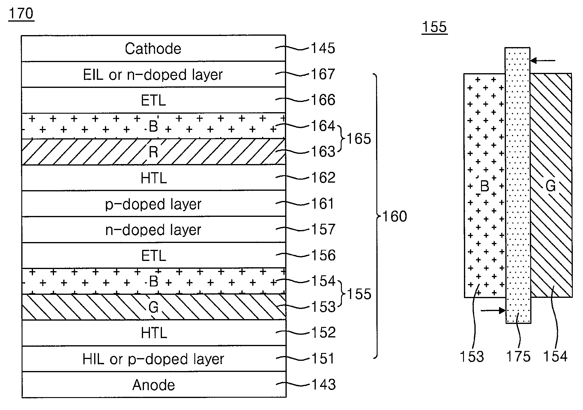
[0048]Referring to the FIG. 3, the stacked structure of the white organic light emitting cell 170 in accordance with the present invention includes an anode 143, a first emissive layer 155, first and second intermediate layers 157 and 161, a second emissive layer 165, and a cathode 145.

[0049]The first emissive layer 155 has a structure in which a first sub-emissive layer 153 of green (G) and a second sub-emissive layer 154 of blue (B) are stacked, and the second emissive layer 165 has a structure in which a third sub-emissive layer 163 of red (R) and a fourth sub-emissive layer 164 of blue (B) are stacked.

[0050]The first and second intermediate layers 157 and 161 are formed between the first emissive layer 155 and the second emissive layer 165. The first intermediate layer 157 supplies electrons to the first emissive layer 155, and the second intermediate layer 161 supplies holes to the second emissive layer 165.

[0051]Such first and second intermediate layers 157 and 161 may be form...

second embodiment

[0059]Referring to the FIG. 4, the stacked structure of the white organic light emitting cell 170 in accordance with the present invention includes an anode 143, a first emissive layer 155, first and second intermediate layers 157 and 161, a second emissive layer 165, and a cathode 145.

[0060]The first emissive layer 155 has a structure in which a first sub-emissive layer 153 of red (R) and a second sub-emissive layer 154 of blue (B) are stacked, and the second emissive layer 165 has a structure in which a third sub-emissive layer 163 of green (G) and a fourth sub-emissive layer 164 of blue (B) are stacked.

[0061]Since the stacked structure including the first and second intermediate layers 157 and 161, a hole injection layer 151, an electron injection layer 167, first and second hole transport layers 152 and 162, and first and second electron transport layers 156 and 166, and the light emitting mechanism thereof are the same as the first embodiments, their detailed description will b...


PUM


Abstract

A white organic light emitting device includes: an anode formed on a substrate; a first emissive layer, in which a first sub-emissive layer and a second sub-emissive layer are stacked, formed on the substrate; a second emissive layer, in which a third sub-emissive layer and a fourth sub-emissive layer are stacked, formed on the first emissive layer; a first intermediate layer supplying electrons to the first emissive layer and a second intermediate layer supplying holes to the second emissive layer, wherein the first and second intermediate layers are formed between the first emissive layer and the second emissive layer; and a cathode formed on the second emissive layer.

Description

CROSS-REFERENCE TO RELATED APPLICATION[0001]This application claims priority to and the benefit of Korean Patent Application No. 10-2007-0024027, filed on Mar. 12, 2007, the disclosure of which is incorporated herein by reference in its entirety.BACKGROUND OF THE INVENTION[0002]1. Field of the Invention[0003]The present invention relates to a white organic light emitting device and, more particularly, to a white organic light emitting device which includes first and second emissive layers each having a blue emissive layer to improve the light emission efficiency.[0004]2. Description of the Related Art[0005]Image display devices that are thinner, lighter and more portable and that employ organic light emitting displays (OLED), have attracted much attention. The OLED has the advantage that it can be manufactured paper-thin, with a light emitting element using a thin emissive layer between electrodes.[0006]The OLED includes an anode transmitting light, a cathode reflecting light, and a...

Claims


Application Information

Patent Timeline
Patent Type & Authority Patents(United States)
IPC IPC(8): H01J1/62H01J63/04
CPCH01L51/5036H01L51/5278H10K50/125H10K50/19H05B33/14
Inventor CHOI, JUN-HOHA, JAE-KOOKKIM, SEONG-MIN
Owner SAMSUNG DISPLAY CO LTD
Why Eureka
Try Eureka