Supercharge Your Innovation With Domain-Expert AI Agents!

Liquid crystal display panel with spherical spacer and a concave portion opposite to the spacer

a liquid crystal display and spacer technology, applied in non-linear optics, instruments, optics, etc., can solve the problems of reducing the design margin for superposing two substrates opposite to each other, affecting the uniform and precise superposition of two substrates in the wide region of the whole substrate, and affecting the appearance quality. , to achieve the effect of convenient alignment, convenient alignment and sufficient friction resistance at the time of conta

Inactive Publication Date: 2010-10-12
NEC LCD TECH CORP
View PDF12 Cites 2 Cited by
  • Summary
  • Abstract
  • Description
  • Claims
  • Application Information

AI Technical Summary

Benefits of technology

"The present invention provides an LCD panel with a pair of substrates that hold a liquid crystal layer therebetween. The substrates can be easily aligned and misalignment during transportation or curing can be suppressed. This is achieved by fixing a spherical spacer to one of the substrates and forming a concave portion in the other substrate. The concave portion has a side wall portion inclined at a predetermined angle to the plane of the substrate and a cross-section of the concave portion in a direction perpendicular to the substrate is V-shaped. An insulating film is formed in the concave portion and the concave portion penetrates the insulating film. The invention also provides a method of manufacturing the LCD panel. The technical effects of the invention include easy alignment of the substrates and prevention of light leakage due to misalignment."

Problems solved by technology

When the degree of precision in the superposing two substrates is below the standard, light is not shielded from entering the alignment defective regions and the alignment defective regions where light is not shielded from entering, glows at the time of black display, thereby causing display defect.
In particular, as a substrate is recently becoming larger, it is becoming more difficult to superpose two substrates opposite to each other uniformly and precisely in wide regions of the whole substrates.
In addition, due to the demand for further fineness, a design margin for superposing two substrates opposite to each other becomes smaller, and the above-described problem becomes more obvious.

Method used


Image

  • Liquid crystal display panel with spherical spacer and a concave portion opposite to the spacer
  • Liquid crystal display panel with spherical spacer and a concave portion opposite to the spacer
  • Liquid crystal display panel with spherical spacer and a concave portion opposite to the spacer

Examples


Embodiment Construction

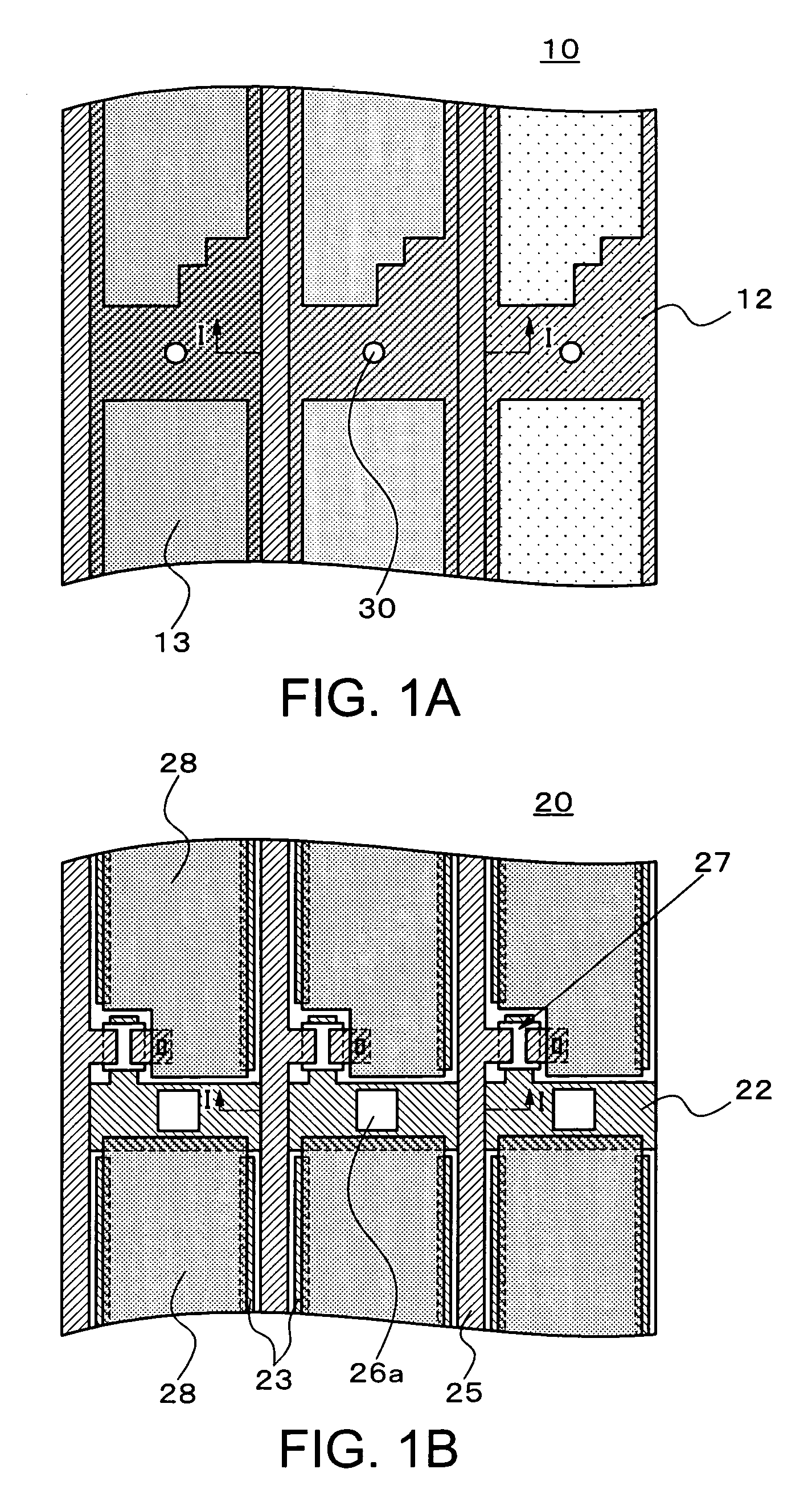
[0050]Before describing preferred embodiments of the present invention, an LCD panel of the related art will be described in detail. Firstly, a cell gap control structure of a first related art will be described. In Japanese Patent Application Laid-open No. 2003-121859, proposed is an LCD panel as shown in FIG. 8. In the LCD panel, columnar spacers 51 are provided on a CF substrate 50 and apertures 53a are provided in an interlayer insulating film 53 in a TFT substrate 52. The interlayer insulating film 53 is formed of an organic material, and each of the apertures 53a is located so as to correspond a position of the columnar spacer 51. Each of the columnar spacers 51 is supported by a contact portion 51a of the columnar spacer 51 within the corresponding aperture 53a, so that defects such as abnormal display are prevented, which are easily caused when the cell gap locally expands under a high temperature.

[0051]Moreover, a cell gap control structure of a second related art will be d...


PUM

PropertyMeasurementUnit
angleaaaaaaaaaa
areaaaaaaaaaaa
photosensitiveaaaaaaaaaa

Abstract

A spherical spacer is used as a spacer member defining a gap, and is fixed to a color filter substrate. A concave portion coming in contact with a part of the spherical spacer is formed in a position in a TFT substrate, the position being opposite to the spherical spacer. The substrates are bonded with each other by engaging the spherical spacer and the concave portion with each other.

Description

BACKGROUND OF THE INVENTION[0001]1. Field of the Invention[0002]The present invention relates to a liquid crystal display (LCD) panel and a method of manufacturing the same, and particularly relates to an LCD panel capable of achieving excellent control of a cell gap and a method of manufacturing the same.[0003]2. Description of the Related Art[0004]As a display device of Audio and Visual (AV) equipment or Office Automation (OA) equipment, an LCD device is widely used due to its advantages such as a thin shape, a light weight and low power consumption. This LCD device includes an LCD panel in which a liquid crystal layer is held between a first substrate and a second substrate. On the first substrate, switching elements such as Thin Film Translators (TFT) are formed in a matrix form (hereinafter referred to as a TFT substrate), and on the second substrate, a color filter (CF), a black matrix (BM) and the like are formed (hereinafter referred to as a CF substrate). By controlling an ...

Claims


Application Information

Patent Timeline
Patent Type & Authority Patents(United States)
IPC IPC(8): G02F1/1333G02F1/1335G02F1/1339
CPCG02F1/13394
Inventor HASHIMOTO, YOSHIAKI
Owner NEC LCD TECH CORP
Features
  • R&D
  • Intellectual Property
  • Life Sciences
  • Materials
  • Tech Scout
  • Unparalleled Data Quality
  • Higher Quality Content
  • 60% Fewer Hallucinations
Learn More