

Switching amplifiers
a technology of switching amplifier and amplifier, which is applied in the direction of amplifier with negative feedback circuit arrangement, dc isolation amplifier, amplifier with semiconductor device/discharge tube, etc., can solve the problems of poor optimal circuit performance, power output limitation, and inability to achieve good switching characteristics of p-channel devices that operate above 100 v
- Summary
- Abstract
- Description
- Claims
- Application Information
AI Technical Summary
Benefits of technology
Problems solved by technology
Method used
Image

Examples
Embodiment Construction
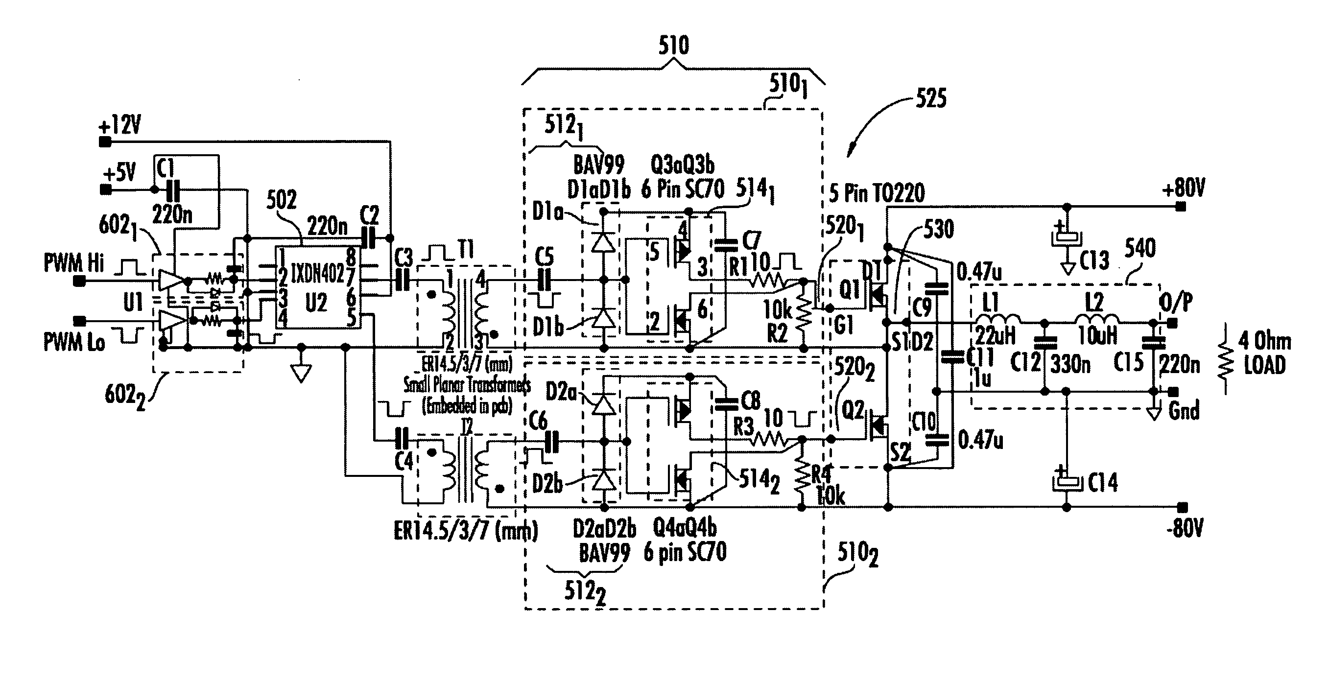
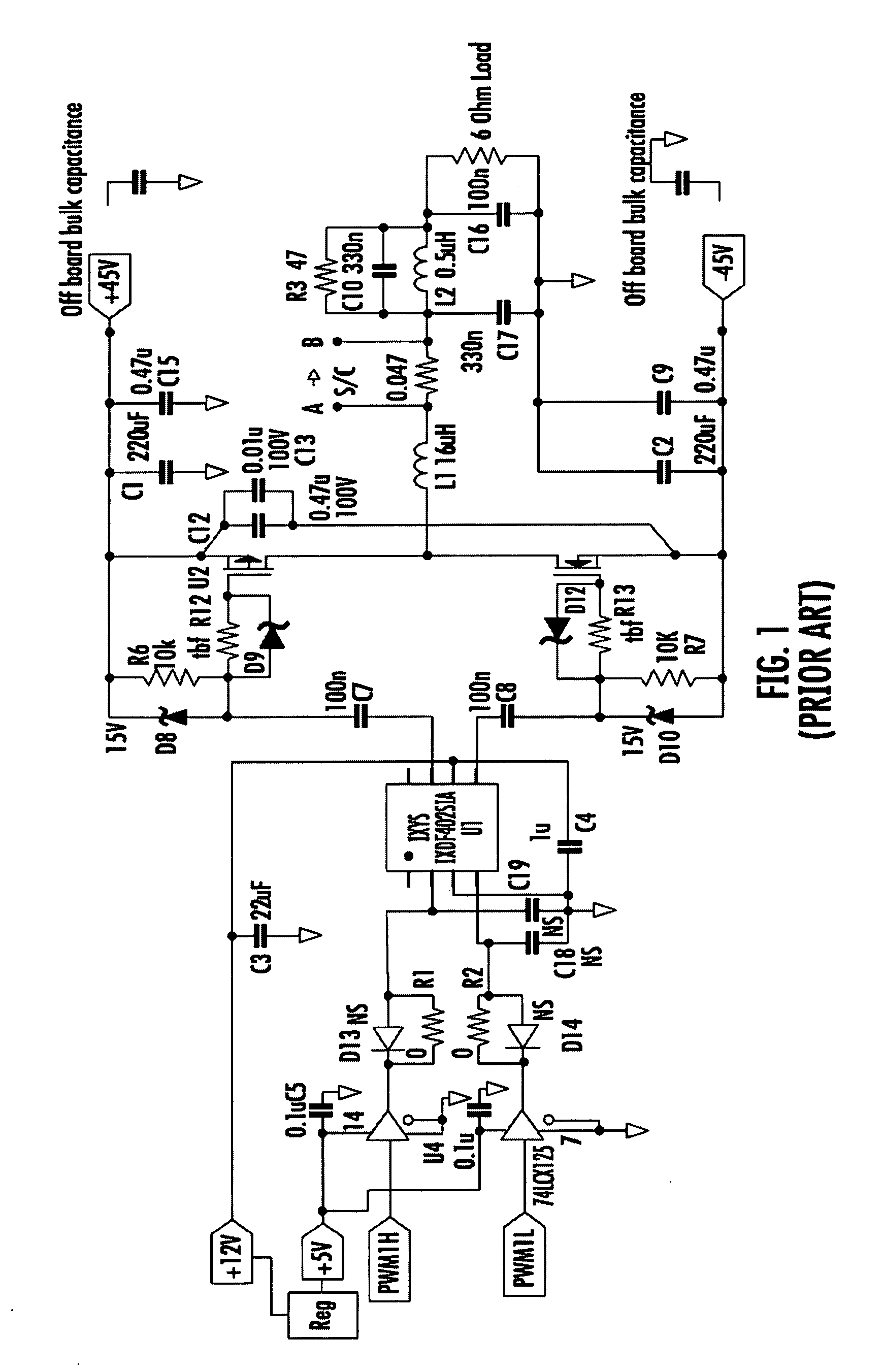
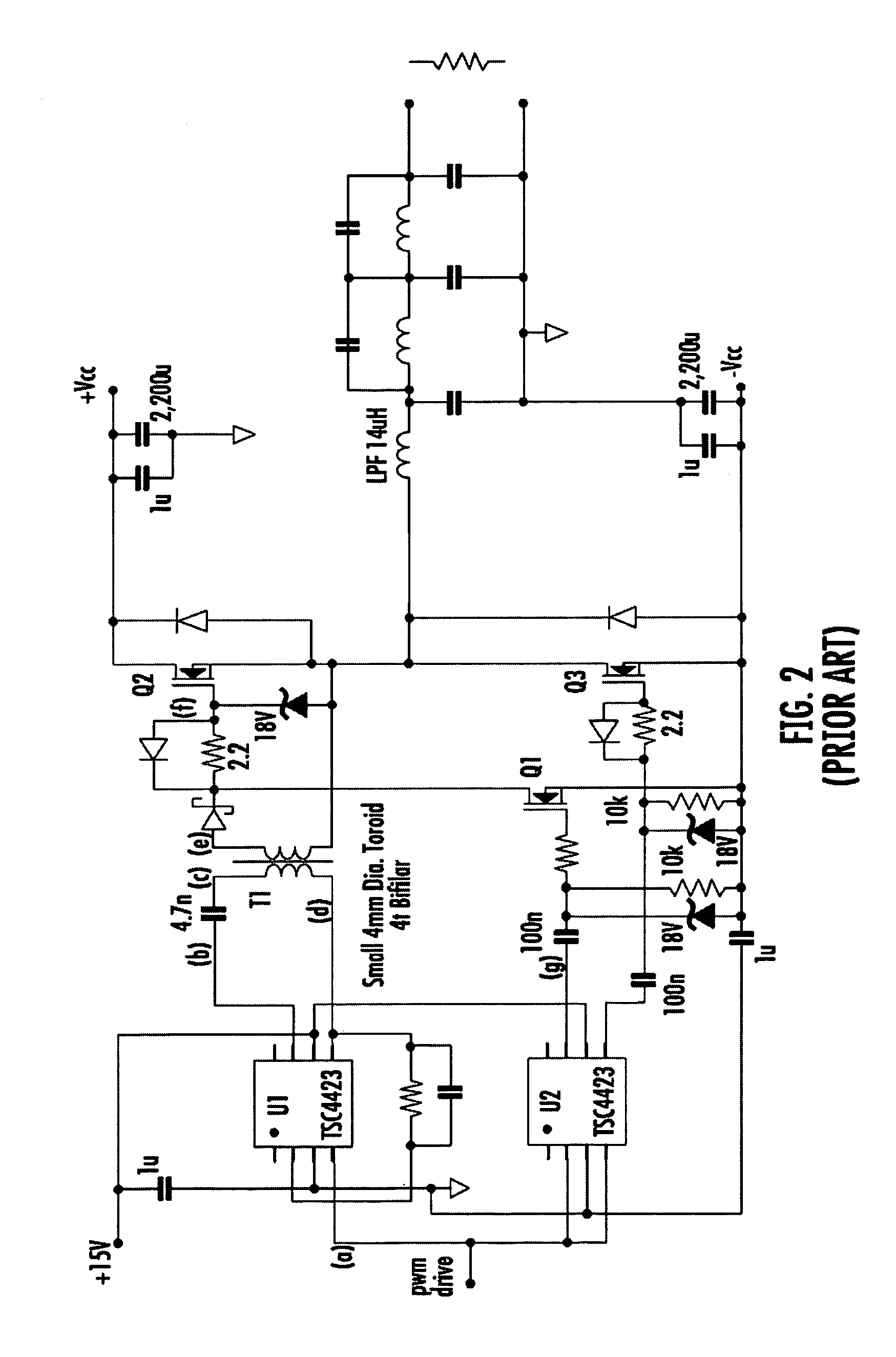
[0012]A switching amplifier typically includes a pair of switching output devices (e.g., MOSFETs) that are turned on and off by drivers. It is important that such switching output devices not be on, or in conduction, at the same time, as high current will flow between voltage supply rails and through the switching output devices, causing a lack of efficiency, and potentially destruction of the devices. A dead time, which is a time when neither switching output device is turned on, is used to guarantee this does not occur. However, such dead time, if too long, can result in high total harmonic distortion plus noise (THD+N) and low efficiency. Embodiment of the present invention generally relate to audio amplification systems and more particularly to systems and methods for reducing and preferably minimizing distortion and noise resulting from such dead time.
[0013]An embodiment of the present invention provides a method whereby the output switching semiconductors (switches) have a rel...
PUM
 Abstract
Description
Claims
Application Information