Package-on-package device, semiconductor package and method for manufacturing the same

Active Publication Date: 2010-11-23
ADVANCED SEMICON ENG INC
View PDF5 Cites 66 Cited by
  • Summary
  • Abstract
  • Description
  • Claims
  • Application Information

AI Technical Summary

Benefits of technology

[0012]According to the POP device of the embodiment of the prevent invention, the interposer can provide the bottom and top packages with electrical connection, and the interposer can provide more functions.

Problems solved by technology

However, the conventional POP device has not any interposer or substrate which is disposed between the top and bottom packages 20, 10 for providing the electrical connection or more functions.

Method used


Image

  • Package-on-package device, semiconductor package and method for manufacturing the same
  • Package-on-package device, semiconductor package and method for manufacturing the same
  • Package-on-package device, semiconductor package and method for manufacturing the same

Examples


Embodiment Construction

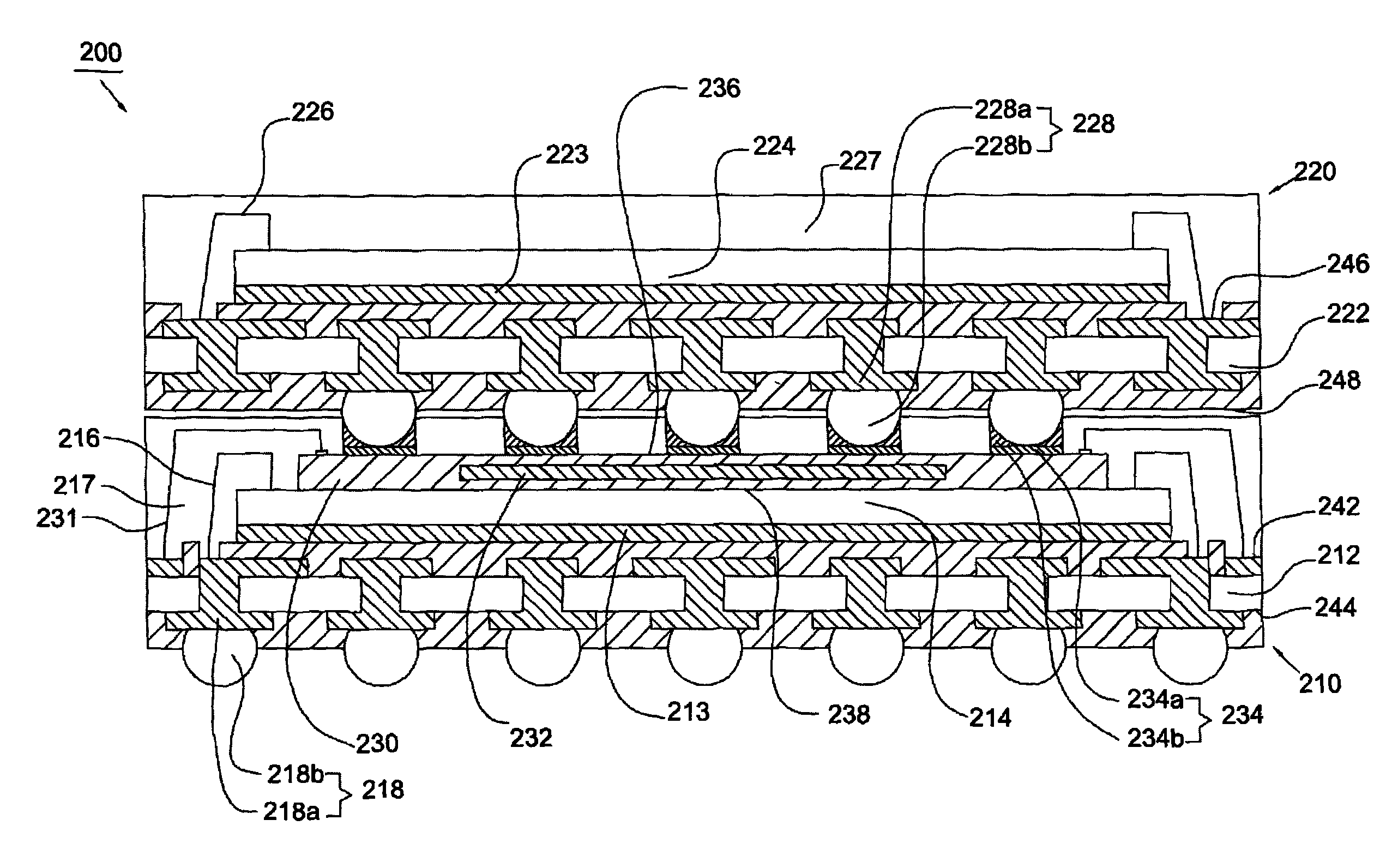
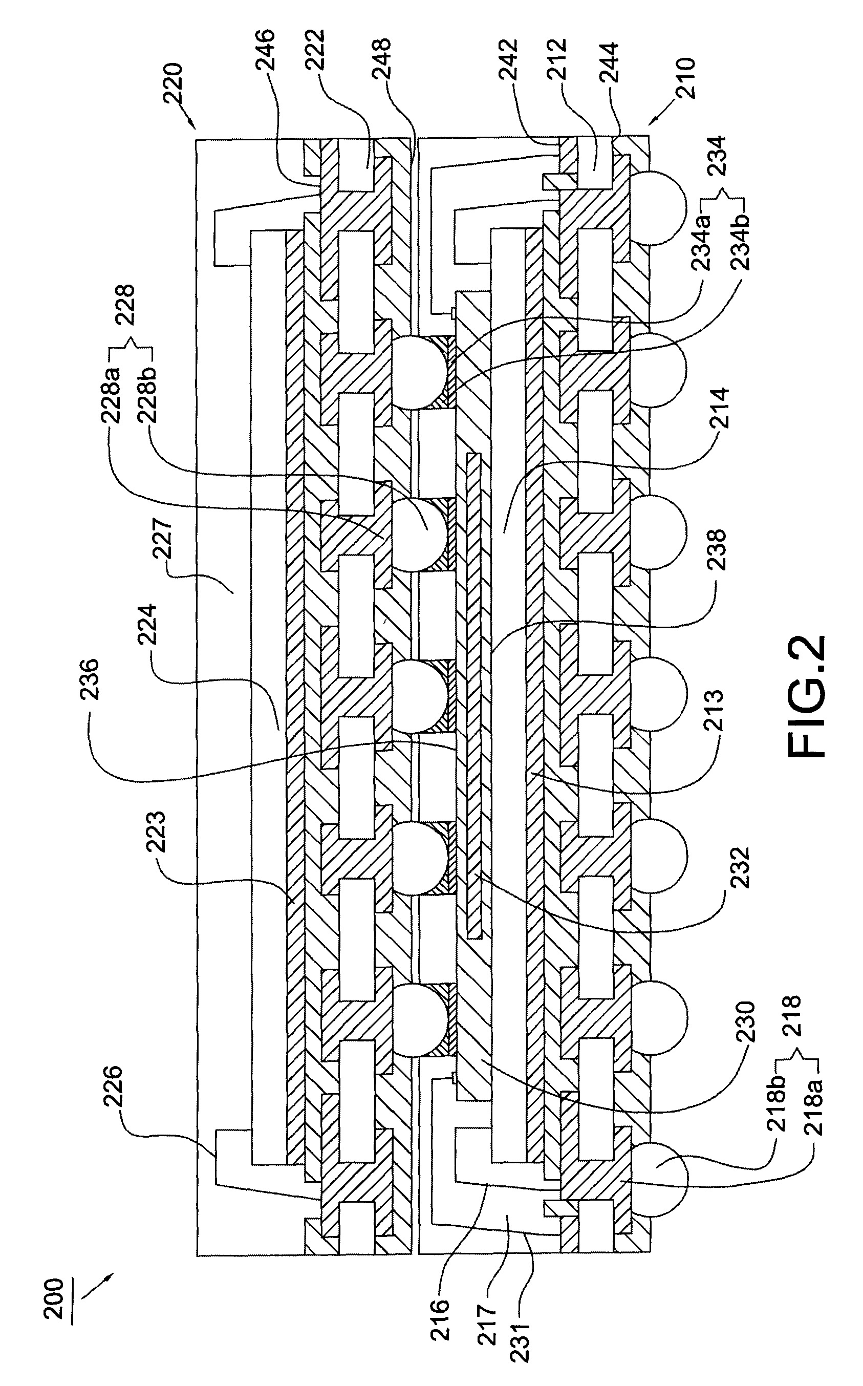
[0019]Referring to FIG. 2, it depicts a stacked package (i.e. package-on-package, POP) device 200 according to an embodiment of the present invention. The POP device 200 includes a top package 220 and a bottom package 210.

[0020]The bottom package 210 includes a first chip 214 mounted and electrically connected to an upper surface 242 of a first substrate 212. The first substrate 212 of the bottom package 210 has upper and lower metal layers which can be patterned to provide appropriate circuitry and electrically connected by way of vias. An interposer 230 is disposed on the first chip 214 and electrically connected to the upper surface 242 of the first substrate 212. Referring to FIG. 3, the interposer 230 can be a multi-layer circuit substrate or a silicon substrate with circuit formed therein. For example, a silicon substrate 130 has an upper surface 136 and a lower surface 138. An embedded component 232 is disposed within an opening 132 of the silicon substrate 130 and secured by...


PUM


Abstract

A semiconductor package includes a substrate, a chip, an interposer and a molding compound. The chip is electrically connected to the upper surface of the substrate. The interposer is disposed on the chip, and electrically connected to the upper surface of the substrate. The interposer includes an embedded component and a plurality of electric contacts, wherein the embedded component is located between the upper and lower surfaces of the interposer, and the electric contacts are located on the upper surface of the interposer. The molding compound seals the chip and covers the upper surface of the substrate and the lower surface of the interposer.

Description

CROSS REFERENCE TO RELATED APPLICATION[0001]This application claims the priority benefit of Taiwan Patent Application Serial Number 097146551, filed on Dec. 1, 2008, the full disclosure of which is incorporated herein by reference.BACKGROUND OF THE INVENTION[0002]1. Field of the Invention[0003]The present invention generally relates to a stacked package device, and more particularly to a bottom package of a stacked package device including an interposer.[0004]2. Description of the Related Art[0005]Currently, a package-on-package (hereinafter referred to as POP) device is related to a semiconductor package disposed on another semiconductor package. The basic object of the POP device is to increase the density of components so as to result in more functions of components per unit volume and better regional efficiency. Thus, the total area of the POP device can be decreased, and the cost is reduced simultaneously.[0006]FIG. 1 is a diagrammatic sketch in a sectional view illustrating th...

Claims


Application Information

Patent Timeline
Patent Type & Authority Patents(United States)
IPC IPC(8): H01L21/00
CPCH01L23/49833H01L25/0657H01L25/105H01L25/16H01L23/3128H01L24/48H01L2224/48091H01L2224/48095H01L2224/48227H01L2224/73265H01L2225/0651H01L2225/06575H01L2924/15311H01L2924/1532H01L2924/15331H01L2924/19041H01L2924/19107H01L2924/00014H01L2224/32225H01L2924/1815H01L2924/00012H01L2225/1023H01L2225/1041H01L2225/1058H01L2924/181H01L24/73H01L2224/45099H01L2224/45015H01L2924/207
Inventor YU, LIN WANGWENG, CHENG YI
Owner ADVANCED SEMICON ENG INC
Why Eureka
Try Eureka