

Method for detecting tip position of probe, alignment method, apparatus for detecting tip position of probe and probe apparatus
a technology the apparatus for detecting the tip position of the probe, which is applied in the direction of instruments, semiconductor/solid-state device testing/measurement, measurement devices, etc. it can solve the problems of large time-consuming alignment of the object, the probe may not be able to make close contact with the respective electrode pads in their entirety, and the production quality of the probe card is affected, so as to achieve the effect of increasing inspection reliability
- Summary
- Abstract
- Description
- Claims
- Application Information
AI Technical Summary
Benefits of technology
Problems solved by technology
Method used
Image

Examples
Embodiment Construction
[0045]Hereinafter, embodiments of the present invention will be described with reference to FIGS. 1 to 6.
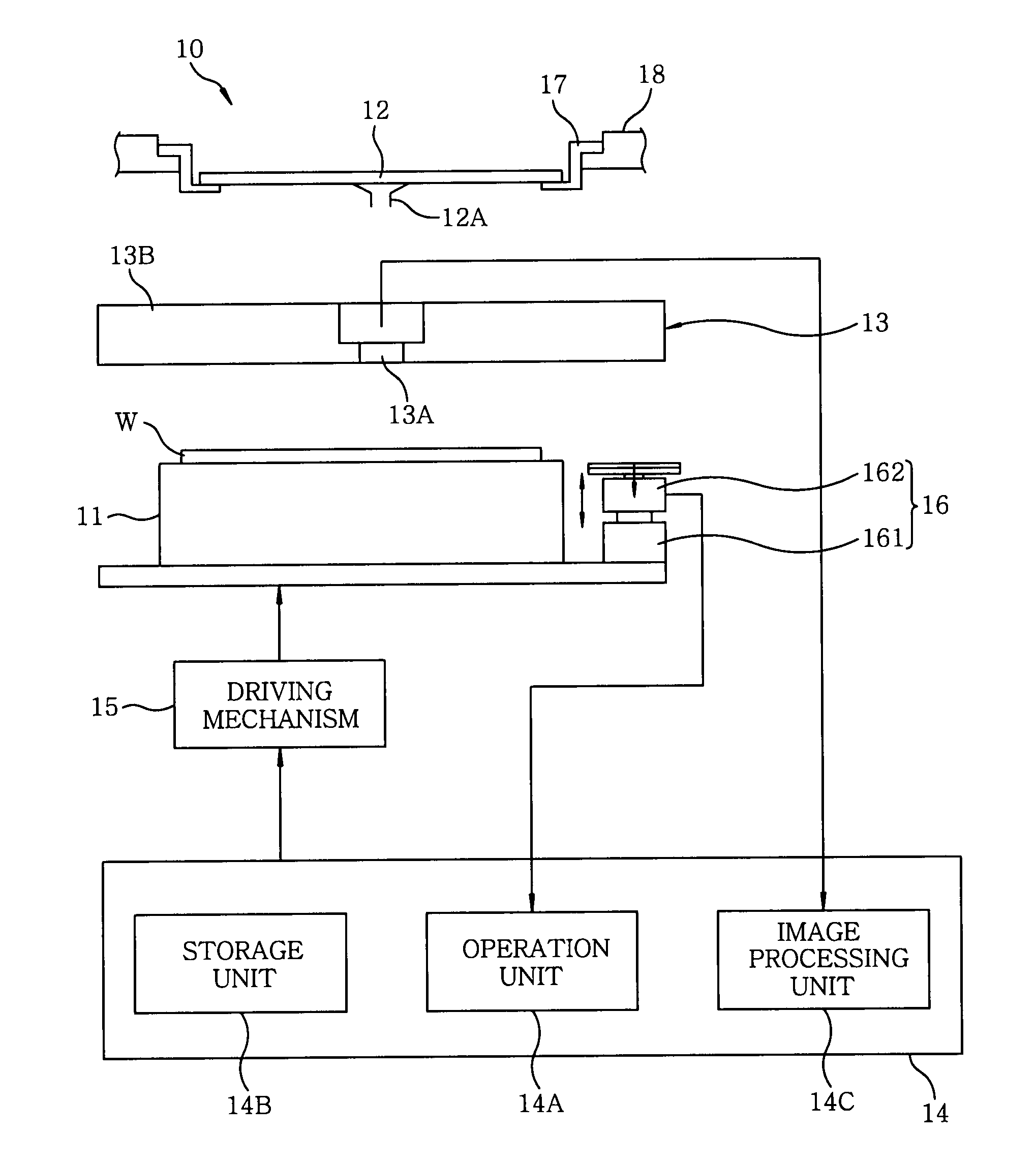
[0046]First, a probe apparatus in accordance with an embodiment of the present invention will be described, e.g., with reference to FIG. 1. As shown in FIG. 1, the probe apparatus 10 of the present embodiment includes a movable wafer chuck 11 for mounting a semiconductor wafer W to be inspected thereon, a probe card 12 arranged above the wafer chuck 11, an alignment mechanism 13 for aligning a plurality of probes 12A of the probe card 12 with the semiconductor wafer W mounted on the wafer chuck 11, and a control unit 14 for controlling the wafer chuck 11, the alignment mechanism 13 and the like. Under the control of the control unit 14, the alignment mechanism 13 is driven to align the semiconductor wafer W mounted on the wafer chuck 11 and the probes 12A of the probe card 12. Subsequently, electrical characteristics inspection of the semiconductor wafer W is conducted by brining...
PUM
 Abstract
Description
Claims
Application Information