Thermoplastic resin composition for semiconductor, adhesion film, lead frame, and semiconductor device using the same, and method of producing semiconductor device

a technology of adhesion film and semiconductor, which is applied in the direction of film/foil adhesive, heat-activated film/foil adhesive, semiconductor/solid-state device details, etc., can solve the problems of thermal damage of semiconductor elements, deterioration of the reliability of semiconductor packages, and unfavorable use of them

Inactive Publication Date: 2010-11-30
RESONAC CORPORATION
View PDF11 Cites 5 Cited by
  • Summary
  • Abstract
  • Description
  • Claims
  • Application Information

AI Technical Summary

Benefits of technology

[0006]In view of the circumstances above, an object of the present invention is to provide an adhesion film for semiconductor that allows tight adhesion between the lead frame and a semiconductor chip at a bonding temperature lower than that with a traditional polyimide resin without generation of voids and can be used for protection of the lead frame-exposed area, a thermoplastic resin composition for semiconductor used as an adhesive agent layer of the adhesion film, and a lead frame, semiconductor device having the adhesion film and a method of producing a semiconductor device.
[0031]With the thermoplastic resin composition for semiconductor according to the present invention and the adhesion film for semiconductor using the same, it is possible to bond the lead frame and a semiconductor chip tightly to each other at a bonding temperature lower than that with a traditional polyimide resin without generation of voids. The lead frame and the semiconductor device having the adhesive film according to the present invention are superior in wire-bonding efficiency, reflow resistance, and reliability.
[0032]The adhesion film for semiconductor according to the present invention is favorably used in applications for protection of the exposed region of various surface-treated lead frames, and it is possible to produce a semiconductor device having a structure in which the lead frame exposed on the rear face is used as a lead terminal that is advantageous in increasing density and reducing area and thickness at high processability and productivity.

Problems solved by technology

However, these adhesives demand heating at higher temperature for an extended period for hardening, and use of them is not favorable from the point of productivity.
In addition, these adhesives, which are relatively more hygroscopic, cause problems such as deterioration in the reliability of semiconductor package.
However, the method demands adhesion at extremely high temperature, which is likely to cause thermal damage in the semiconductor element.
On the other hand, it is possible to decrease the temperature of adhesion by lowering the glass transition temperature of the polyimide resin, but, in such a case, the decrease in glass transition temperature leads to deterioration in heat resistance of the polyimide resin at the same time and easier generation of voids during adhesion, and consequently to deterioration in adhesive strength.
Further, it may also affect the wire-bonding efficiency and the reflow resistance in the production steps for a semiconductor package, consequently leading to deterioration in reliability of the semiconductor package.
The package in such a structure is advantageous for reducing the area and thickness, because the lead frame is not sticking out of the sealing resin, but often causes problems such as migration of sealing resin to the rear face of the lead frame during sealing.
In contrast, the inventors had found that it was possible to prevent the problems above by protecting the lead frame exposed on the rear face with an adhesion film and removing the layer after sealing, but, in recent popularization of various surface treatments such as coating of an organic film on the lead frame surface, there is still a problem of deterioration in the adhesive strength at the interface between the adhesion film and the lead frame.

Method used


Image

  • Thermoplastic resin composition for semiconductor, adhesion film, lead frame, and semiconductor device using the same, and method of producing semiconductor device
  • Thermoplastic resin composition for semiconductor, adhesion film, lead frame, and semiconductor device using the same, and method of producing semiconductor device
  • Thermoplastic resin composition for semiconductor, adhesion film, lead frame, and semiconductor device using the same, and method of producing semiconductor device

Examples


example 1

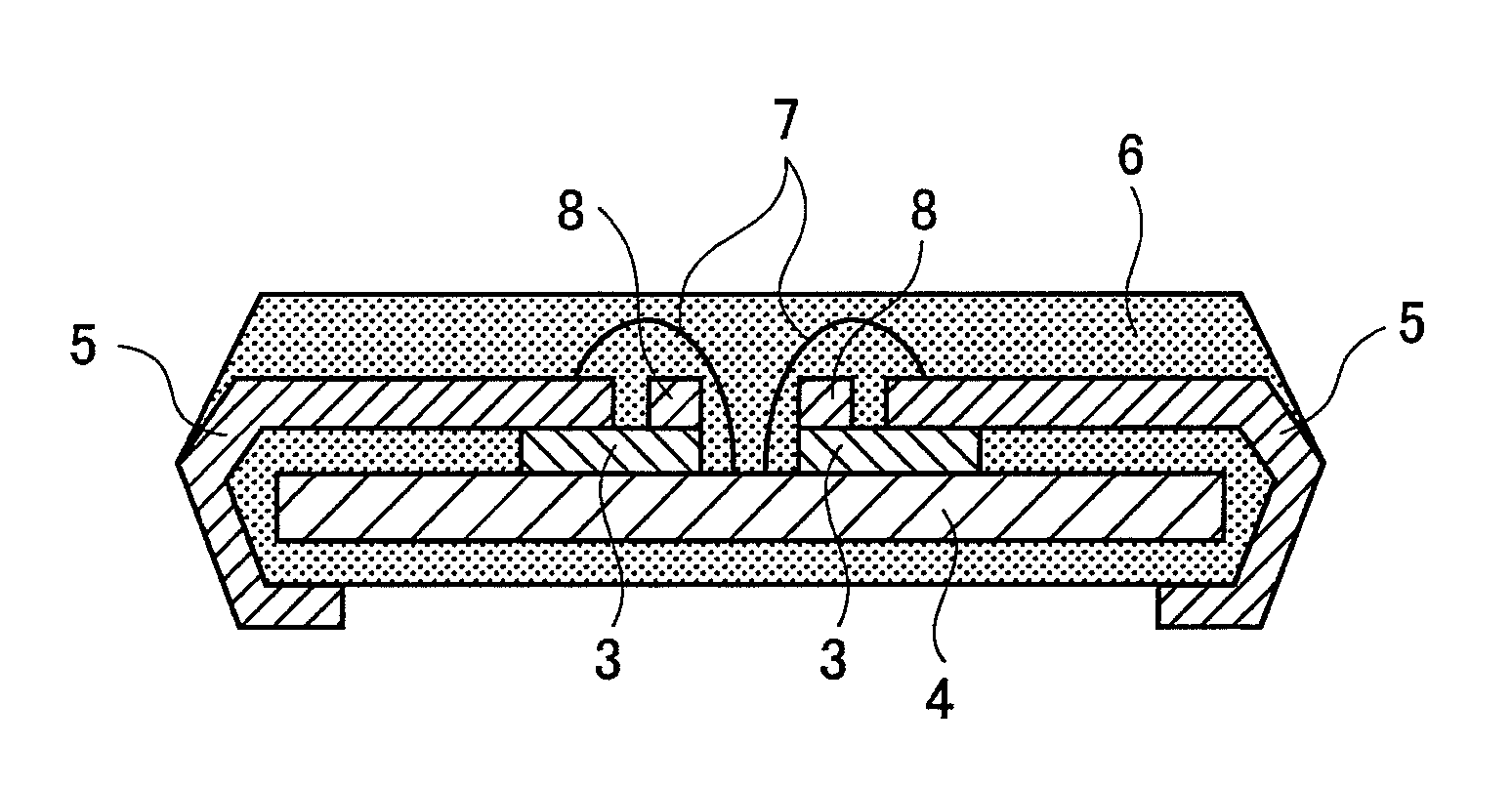
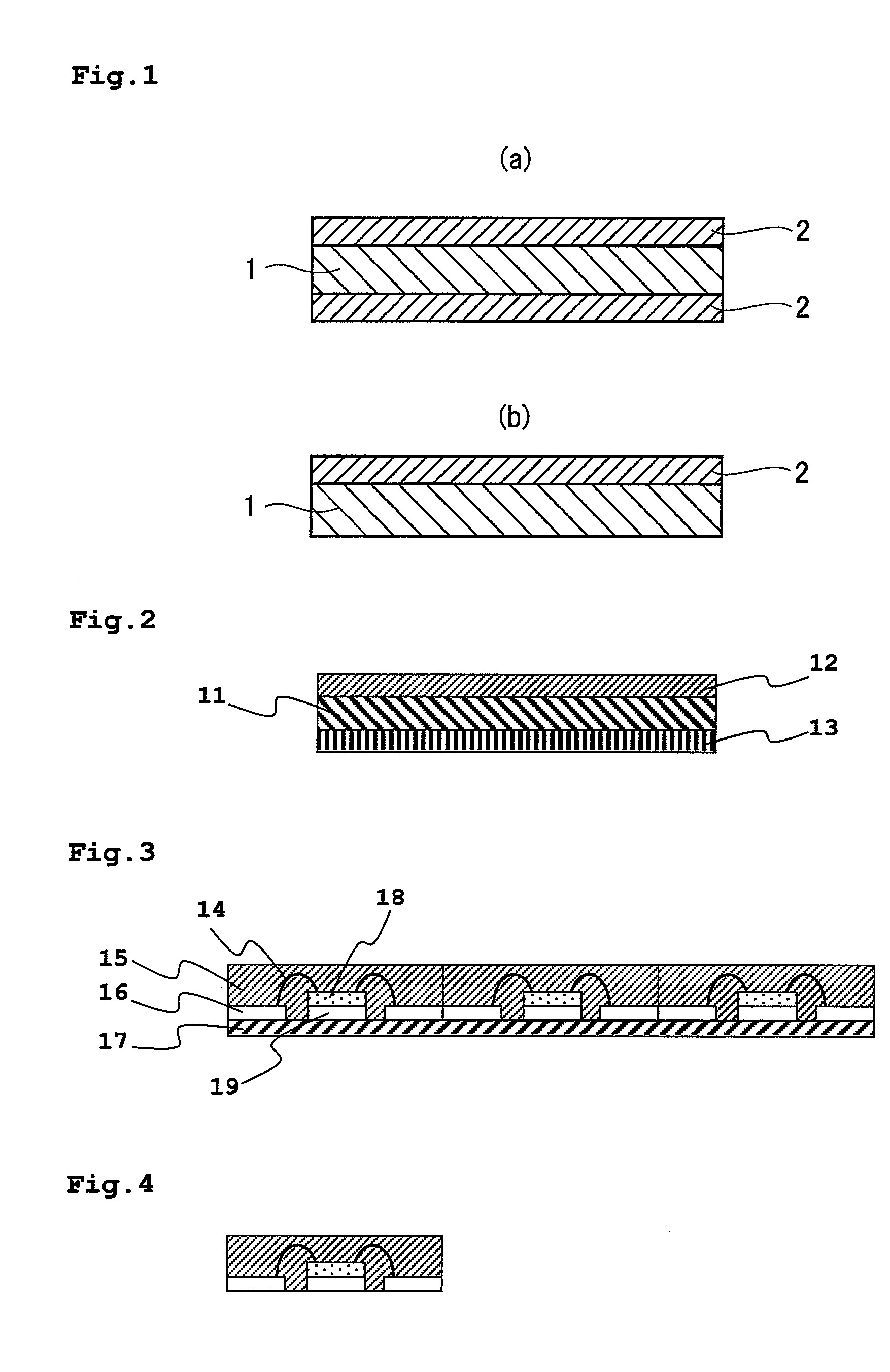
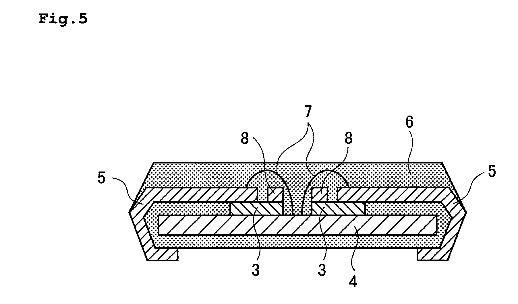
[0102]The thermoplastic resin (A-1) obtained was dissolved in N-methyl-2-pyrrolidone (NMP) uniformly, and a coupling agent (trade name: KBM403, manufactured by Shin-Etsu Silicones Co., Ltd.) was added in an amount of 3 parts with respect to 100 parts of the thermoplastic resin (A-1), to give a resin composition varnish. The nonvolatile matter in the varnish, as determined after heating at 250° C. for 2 hours, was 40%. The varnish was then coated on both faces of a chemically finished polyimide film (trade name: Upilex SPA, manufactured by Ube Industries, Ltd.); dried at 90° C. for 5 minute and additionally at 250° C. for 10 minutes, forming an adhesive agent layer having a thickness of 25 μm, to give an adhesion film for semiconductor in the three-layer structure.

example 2

[0103]An adhesion film for semiconductor in the three-layer structure was prepared in a similar manner to Example 1, except that the thermoplastic resin (A-1) was replaced with the thermoplastic resin (A-2).

example 3

[0104]An adhesion film for semiconductor in the three-layer structure was prepared in a similar manner to Example 1, except that the thermoplastic resin (A-1) was replaced with the thermoplastic resin (A-3) and the coupling agent used was KBM573 (trade name, manufactured by Shin-Etsu Silicones Co., Ltd.).


PUM

PropertyMeasurementUnit
contact angleaaaaaaaaaa
glass transition temperatureaaaaaaaaaa
temperatureaaaaaaaaaa

Abstract

The object of the present invention is to provide an adhesion film for semiconductor that is capable of bonding a semiconductor chip to a lead frame tightly at an adhesion temperature lower than that of the adhesion film of a traditional polyimide resin without generation of voids and that can also be used for protection of lead frame-exposed area, a thermoplastic resin composition for semiconductor for use in the adhesive agent layer therein, and a lead frame having the adhesive film and a semiconductor device; and, to achieve the object, the present invention provides a thermoplastic resin composition for semiconductor, comprising a thermoplastic resin obtained in reaction of an amine component containing an aromatic diamine mixture (A) containing 1,3-bis(3-aminophenoxy)benzene, 3-(3′-(3″-aminophenoxy)phenyl)amino-1-(3′-(3″-aminophenoxy)phenoxy)benzene and 3,3′-bis(3″-aminophenoxy)diphenylether, and an acid component (C), an adhesion film for semiconductor using the same, a lead frame having the adhesion film and a semiconductor device using the same.

Description

TECHNICAL FIELD[0001]The present invention relates to a thermoplastic resin composition favorable for use as a semiconductor mounting material for electronic applications, an adhesion film for semiconductor and a semiconductor device.BACKGROUND ART[0002]Recently, there are proposed some semiconductor-mounting methods compatible with the demand for increase in performance and density of semiconductor elements and in mounting density. Typical of them are a COL (chip on lead) method of mounting a semiconductor chip on a lead frame having no die pad and a LOC (lead on chip) method of mounting a lead on a semiconductor chip.[0003]Paste adhesive agents of a epoxy-based or acrylic resin and heat-resistant materials carrying a coated adhesive agent are commonly used as adhesive materials for bonding a semiconductor element on lead frame in these methods. However, these adhesives demand heating at higher temperature for an extended period for hardening, and use of them is not favorable from ...

Claims


Application Information

Patent Timeline
Patent Type & Authority Patents(United States)
IPC IPC(8): C08G73/10C08G73/14C08G69/40C09J7/02C09J177/10B32B15/088H01L21/02H01L23/48C09J179/08C08G69/26C09J177/06C09J7/35
CPCC08G73/106C08L79/08C09J7/0203C09J179/08H01L23/293C08G73/14H01L24/97Y10T428/24959C09J2479/08H01L2924/09701H01L2224/45144Y10T428/2896H01L2224/73215H01L2224/4826H01L2224/48091H01L2224/32245H01L2924/00014H01L2924/00H01L2924/01322H01L2924/15747H01L2924/181H01L2224/97C09J7/35C08G73/02C08G73/10H01L23/50
Inventor TATEOKA, KIYOHIDEKAWAI, TOSHIYASUTANABE, YOSHIYUKINAGOYA, TOMOHIROTOMODA, NAOKO
Owner RESONAC CORPORATION
Why Eureka
Try Eureka