Semiconductor device

a technology of semiconductor devices and semiconductors, applied in semiconductor devices, digital storage, instruments, etc., can solve the problems of limited degree of integration and low reading speed, and achieve the effect of high data retention characteristics and high speed reading ou

Inactive Publication Date: 2010-12-28
RENESAS ELECTRONICS CORP
View PDF22 Cites 18 Cited by
  • Summary
  • Abstract
  • Description
  • Claims
  • Application Information

AI Technical Summary

Benefits of technology

[0018]In view of these circumstances, an object of the present invention is to solve the above problems and provide a technique for realizing a semiconductor device which can perform reading-out at a high speed and has high data retention characteristics.
[0024]According to the present invention, a semiconductor device which can conduct high-speed reading-out and has high data retention characteristics can be realized.

Problems solved by technology

Thus, such a problem arises that a reading speed lowers.
Since the reset operation current is large, such a problem also arises that the degree of integration is limited.

Method used


Image

  • Semiconductor device
  • Semiconductor device
  • Semiconductor device

Examples


first embodiment

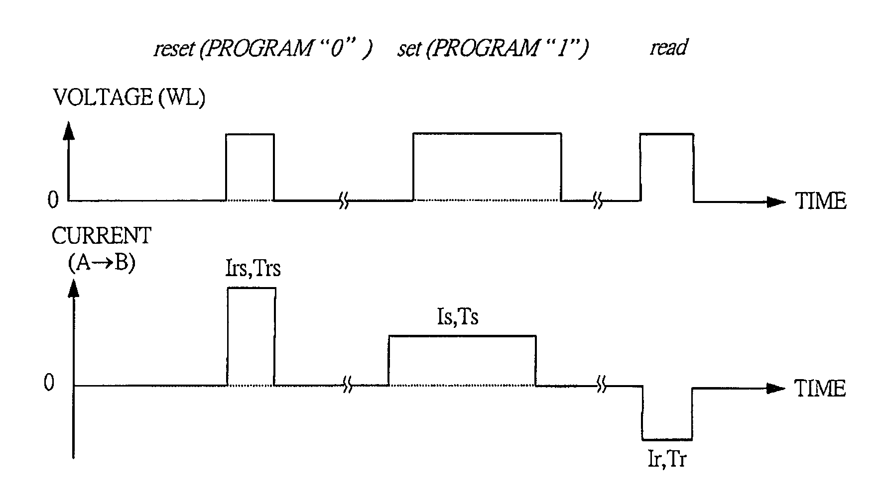
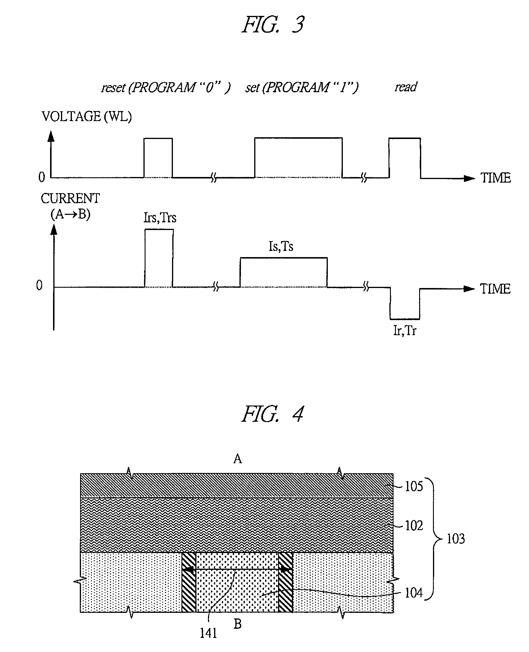
[0070]One example of a phase-change memory cell according to a first embodiment of the present invention will be explained in detail below with reference to FIGS. 4 to 20.

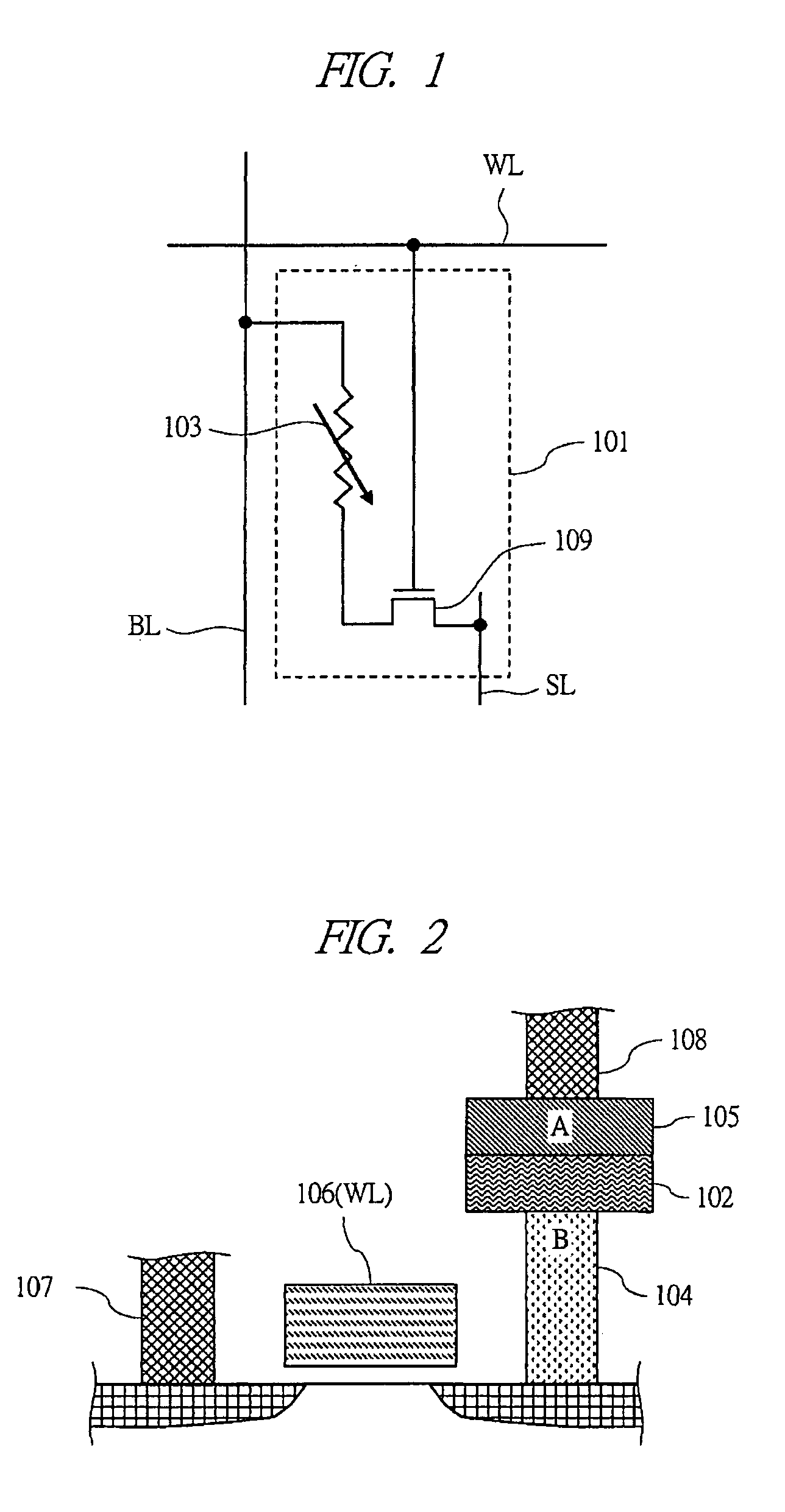
[0071]FIG. 4 shows a cross-sectional structure of an information memory section of a phase-change memory cell. In the information memory section 103, the chalcogenide 102 is sandwiched between the top electrode 105 and the plug electrode 104. A composition of the chalcogenide 102 is Ge2Sb2Te5, and compositions of the plug electrode 104 and the top electrode 105 are tungsten. A size 141 of the plug electrode 104 is a diameter of 160 nm. Note that, the size 141 of the plug electrode 104 may vary according to generation of a semiconductor process to be used. As a composition of the top electrode 105, tungsten is often used, but other conductive materials can be used as the top electrode.

[0072]Experimental results where current has been caused to flow between the top electrode 105 shown by symbol “A” in FIG. 4 and the ...

second embodiment

[0095]One example of a phase-change memory cell according to second embodiment of the present invention will be explained in detail with reference to FIGS. 21 to 26. FIGS. 21 to 23 show layout diagrams of a main portion where respective members configuring a phase-change memory cell are arranged, FIG. 24 shows a cross-sectional view of a main portion taken along line X-X′ in FIGS. 21 to 22, FIG. 25 shows a cross-sectional view of a main portion taken line Y-Y′ in FIGS. 21 to 22, and FIG. 26 shows a layout diagram of main parts of an application example.

[0096]The second embodiment is an example of an application to a structure of a phase-change memory cell with a high integration degree, as will be explained below.

[0097]FIG. 21 shows an active region 303, a source line SL, the word line WL, and a plug electrode 301 contacting a chalcogenide. When a minimum working size is represented by F, a word line spacing is 2F, and a source line spacing is 3F. FIG. 22 shows the active region 303...

third embodiment

[0101]One example of a phase-change memory cell according to a third embodiment of the present invention will be explained in detail with reference to FIGS. 27 and 28. FIGS. 27 and 28 show layout diagrams of a main portion where respective members configuring a phase-change memory cell are arranged.

[0102]The third embodiment is an example where the present invention has been applied to a structure in which both high integration and reliability of a phase-change memory cell are achieved, and it will be explained below.

[0103]FIG. 27 shows an active region 303, a plug electrode 301, and a contact 361 with a source line. Further, a bit line BL and a word line WL are shown in FIG. 28. A word line spacing is 2F and a bit line spacing is 4F. An area of a memory cell is 8F2. Since the structure can take large bit line spacing, such a merit can be obtained that it is easy to conduct the separation of the chalcogenide. Thereby, both high integration and high reliability can be achieved.


PUM


Abstract

A semiconductor device for high-speed reading and which has a high data-retention characteristic is provided. In a semiconductor device including a memory array having a plurality of memory cells provided at intersecting points of a plurality of word lines and a plurality of bit lines, where each memory cell includes an information memory section and a select element, information is programmed by a first pulse (reset operation) for programming information flowing in the bit line, a second pulse (set operation) different from the first pulse, and information is read by a third pulse (read operation), such that the current directions of the second pulse and the third pulse are opposite to each other.

Description

TECHNICAL FIELD[0001]The present invention relates to a semiconductor device, and in particular to an effective technique applied to a high-density integrated memory circuit including a memory cell which discriminates stored information items by utilizing a difference among resistances, for example, a memory cell using phase-change material, a logic-embedded type memory including a memory circuit and a logic circuit provided on the same semiconductor substrate, or a semiconductor device having an analog circuit. In particular, the present invention relates to a high-speed and nonvolatile random access memory which operates with a low voltage.BACKGROUND ART[0002]For example, the growth of a nonvolatile memory market lead by demand for mobile devices, typified by mobile phones, has been significant. A typical example of the nonvolatile memory is a FLASH memory, but since its speed is essentially slow, it is mainly used as a programmable ROM. On the other hand, a high-speed RAM is requ...

Claims


Application Information

Patent Timeline
Patent Type & Authority Patents(United States)
IPC IPC(8): G11C11/00
CPCG11C13/0004G11C13/0069H01L27/24G11C2013/0073G11C2013/0078G11C2213/79H10B63/00
Inventor KUROTSUCHI, KENZOTAKAURA, NORIKATSUFUJISAKI, YOSHIHISA
Owner RENESAS ELECTRONICS CORP
Why Eureka
Try Eureka