Methods for mastering microstructures through a substrate using negative photoresist

a negative photoresist and microstructure technology, applied in the field of microfabricating methods and systems, can solve the problems of difficult to efficiently produce large arrays of optical microstructures with acceptable manufacturing yields, difficult to efficiently produce large arrays of optical microstructures, and many scaling barriers

Active Publication Date: 2011-01-11
BRIGHT VIEW TECHNOLOGIES CORPORATION
View PDF45 Cites 25 Cited by
  • Summary
  • Abstract
  • Description
  • Claims
  • Application Information

AI Technical Summary

Benefits of technology

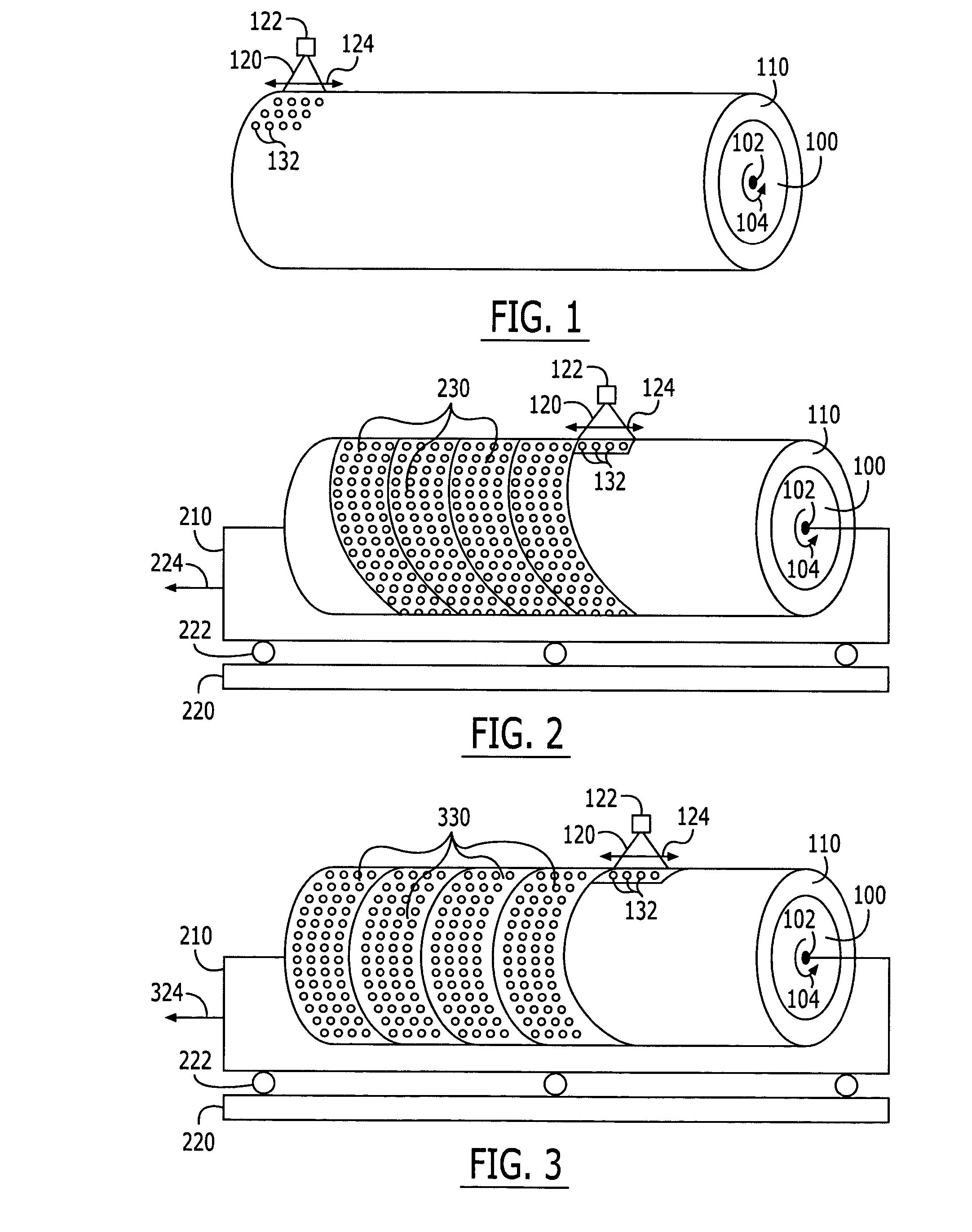
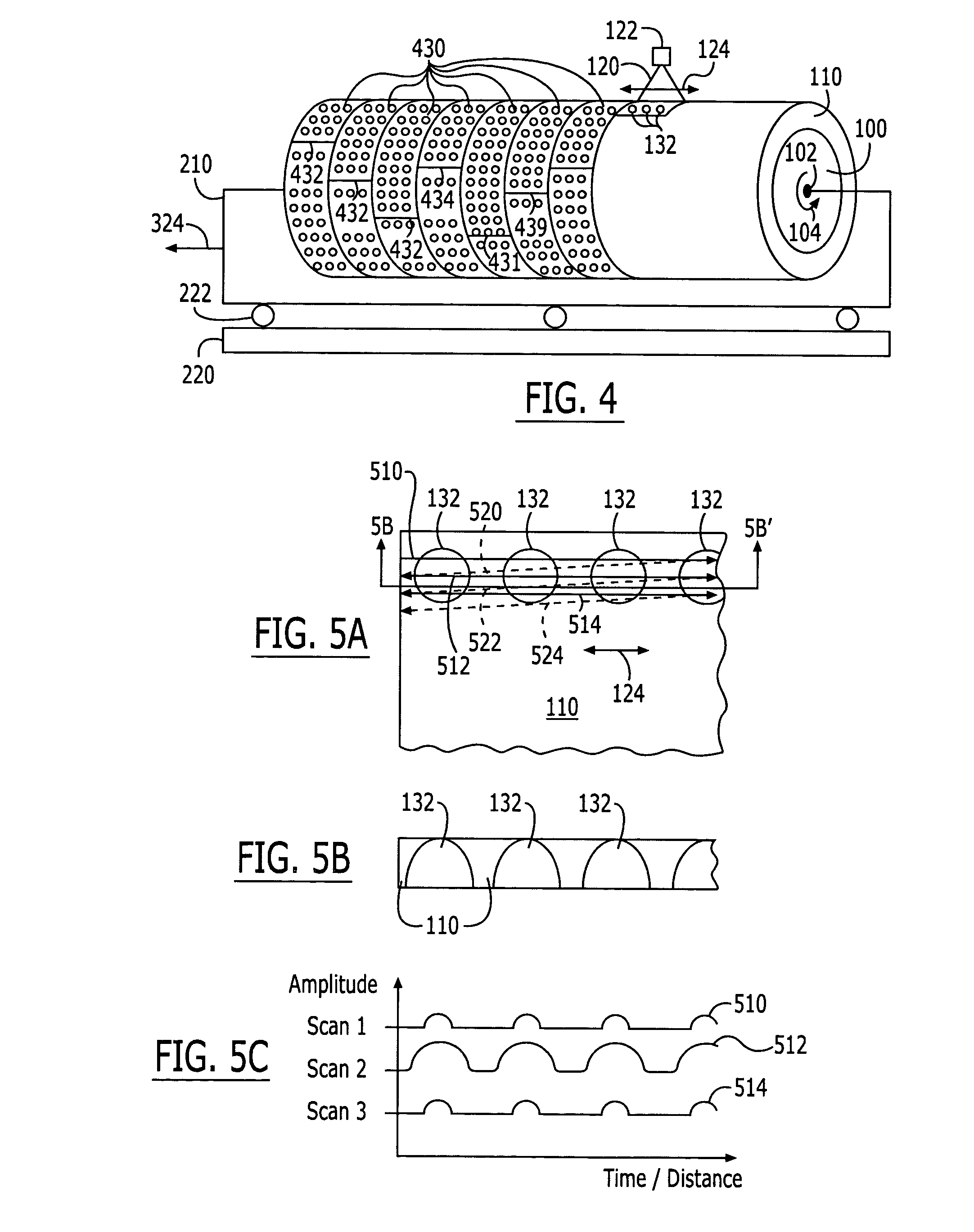
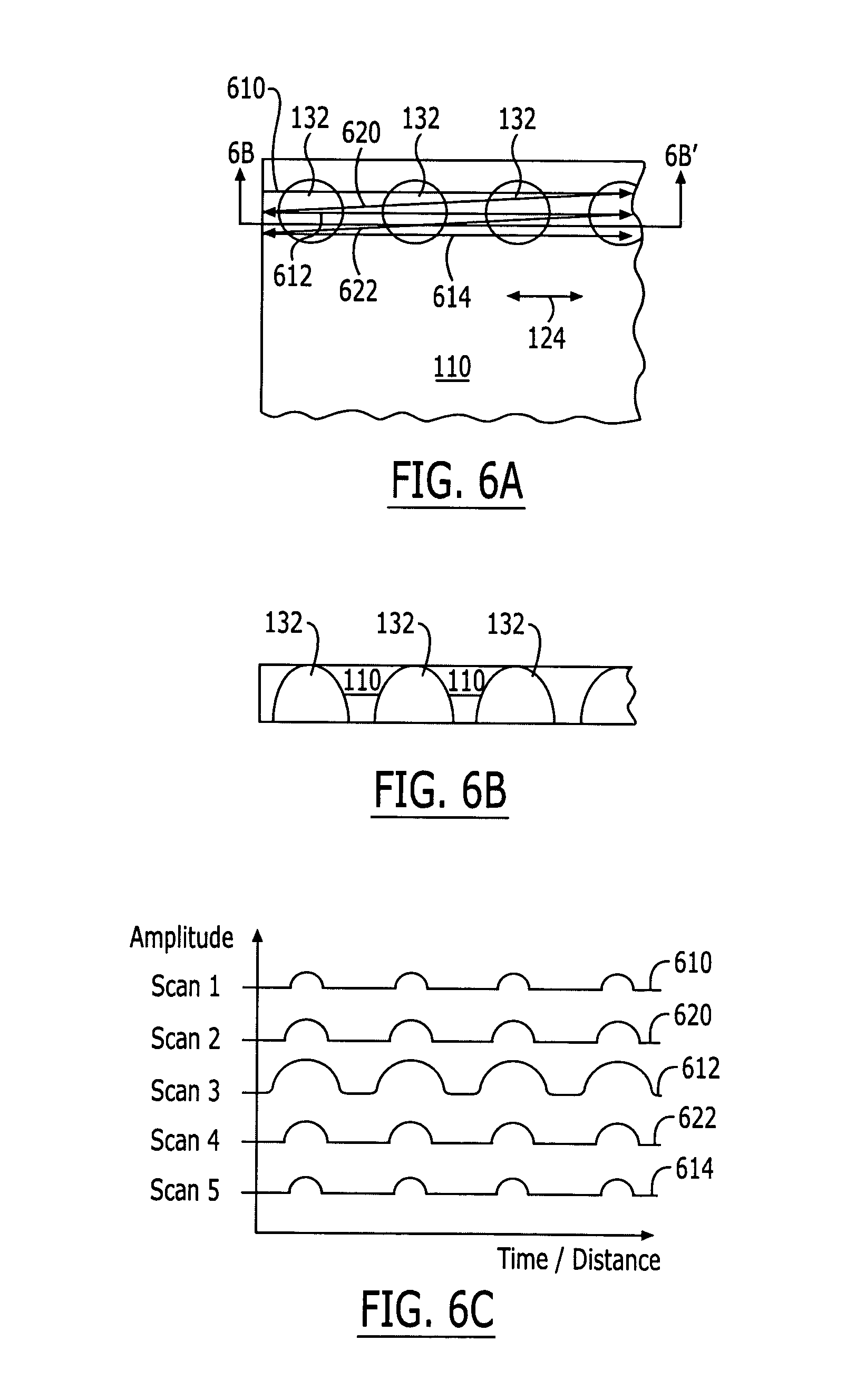
[0009]In some embodiments of the present invention, the negative photoresist layer is thicker than the microstructures, so that when the radiation beam is impinged through the substrate into the negative photoresist layer, an image of buried microstructures is formed in the negative photoresist layer, adjacent the substrate. Moreover, in other embodiments of the present invention, at least some of the microstructures include a base and a top that is narrower than the base, and the imaging is performed through the substrate, to image microstructures in the negative photoresist layer with the bases adjacent the substrate and the tops remote from the substrate. In still other embodiments, the negative photoresist layer is of variable thickness thereacross, and a minimum thickness of the negative photoresist layer is thicker than the microstructures. The radiation beam is impinged through the substrate into the negative photoresist layer, to image buried microstructures in the negative photoresist layer, adjacent the substrate, that are independent of the variable thickness of the negative photoresist layer. In yet other embodiments, the negative photoresist layer includes impurities thereon, remote from the substrate, and the negative photoresist layer is thicker than the microstructures. The radiation beam is impinged through the substrate into the negative photoresist layer, to image buried microstructures in the negative photoresist layer, adjacent the substrate, that are not distorted by the impurities.
[0012]Still other embodiments of the present invention provide microstructure products that include a substrate and a patterned layer of negative photoresist on the substrate, which is patterned to define a plurality of microstructures therein. The negative photoresist is sensitive to radiation at an imaging frequency and the substrate is transparent to the imaging frequency. The microstructures may comprise bases adjacent the substrate and tops remote from the substrate, and / or hemispherical sections as was described above. The substrate may be flexible. The substrate and patterned layer of the negative photoresist can provide a microstructure master.

Problems solved by technology

Unfortunately, however, severe scaling barriers may be encountered in attempting to fabricate large arrays of optical microstructures.
These scaling barriers may make it difficult to efficiently produce large arrays of optical microstructures with acceptable manufacturing yields.
Several barriers may be encountered in attempting to scale optical microstructures to large arrays.
First, the time to master a large array may be prohibitive.
Unfortunately, it may be difficult to produce a master for a large array of optical microstructures within a reasonable time.
For example, calculations may show that it may take years to create a single master for large screen rear projection television.
These mastering times may be prohibitive for viable products.
It also may be difficult to image certain optical microstructures that may be desired for many applications.
However, it may be difficult to master a large array of hemispherical sections using conventional photolithographic techniques.
Finally, it may be difficult to efficiently replicate masters containing large arrays of optical microstructures to produce stampers, so as to enable high volume production of optical microstructure end products for display, television and / or other applications.

Method used


Image

  • Methods for mastering microstructures through a substrate using negative photoresist
  • Methods for mastering microstructures through a substrate using negative photoresist
  • Methods for mastering microstructures through a substrate using negative photoresist

Examples


Embodiment Construction

[0030]The present invention now will be described more fully hereinafter with reference to the accompanying drawings, in which embodiments of the invention are shown. This invention may, however, be embodied in many different forms and should not be construed as limited to the embodiments set forth herein. Rather, these embodiments are provided so that this disclosure will be thorough and complete, and will fully convey the scope of the invention to those skilled in the art. In the drawings, the size and relative sizes of layers and regions may be exaggerated for clarity. Like numbers refer to like elements throughout.

[0031]It will be understood that when an element such as a layer, region or substrate is referred to as being “on” another element, it can be directly on the other element or intervening elements may also be present. Furthermore, relative terms such as “top” or “outer” may be used herein to describe a relationship of one layer or region to another layer or region relat...


PUM

PropertyMeasurementUnit
areaaaaaaaaaaa
sizeaaaaaaaaaa
timeaaaaaaaaaa

Abstract

Microstructures are fabricated by impinging a radiation beam, such as a laser beam, through a substrate that is transparent to the laser beam, into a negative photoresist layer on the substrate. The negative photoresist layer may be subsequently developed to provide a master for optical and / or mechanical microstructures. Related systems, microstructure products and microstructure masters also are disclosed.

Description

CROSS-REFERENCE TO RELATED APPLICATIONS[0001]This application is related to application Ser. No. 10 / 661,916 entitled Systems and Methods for Fabricating Optical Microstructures Using a Cylindrical Platform and a Rastered Radiation Beam to the present inventors, filed concurrently, and application Ser. No. 10 / 661,974, entitled Systems and Methods For Fabricating Microstructures By Imaging A Radiation Sensitive Layer Sandwiched Between Outer Layers, and Microstructures Fabricated Thereby to the present inventors, also filed concurrently, both of which are assigned to the assignee of the present application, the disclosures of both of which are hereby incorporated herein by reference in their entirety as if set forth fully herein.FIELD OF THE INVENTION[0002]This invention relates to microfabricating methods and systems, and more particularly to systems and methods for fabricating microstructures and microstructures fabricated thereby.BACKGROUND OF THE INVENTION[0003]Optical microstruct...

Claims


Application Information

Patent Timeline
Patent Type & Authority Patents(United States)
IPC IPC(8): G03B27/72G02B3/00G02B5/18G03F7/00G03F7/20G03F7/24
CPCB82Y10/00B82Y40/00G02B3/0025G02B5/1857G03F7/0002G03F7/0005G03F7/0007G03F7/0015G03F7/2053G03F7/24G02B3/00G02B5/18G02F7/00G11B7/0025
Inventor FREESE, ROBERT P.RINEHART, THOMAS A.WOOD, ROBERT L.
Owner BRIGHT VIEW TECHNOLOGIES CORPORATION
Why Eureka
Try Eureka