Semiconductor memory device

a memory device and semiconductor technology, applied in the direction of semiconductor devices, basic electric elements, electrical appliances, etc., can solve the problem of higher leakage curren

Inactive Publication Date: 2011-01-11
BESANG
View PDF51 Cites 220 Cited by
  • Summary
  • Abstract
  • Description
  • Claims
  • Application Information

AI Technical Summary

Problems solved by technology

Using the smaller pattern size induces problems like higher leakage current.

Method used


Image

  • Semiconductor memory device
  • Semiconductor memory device
  • Semiconductor memory device

Examples


Embodiment Construction

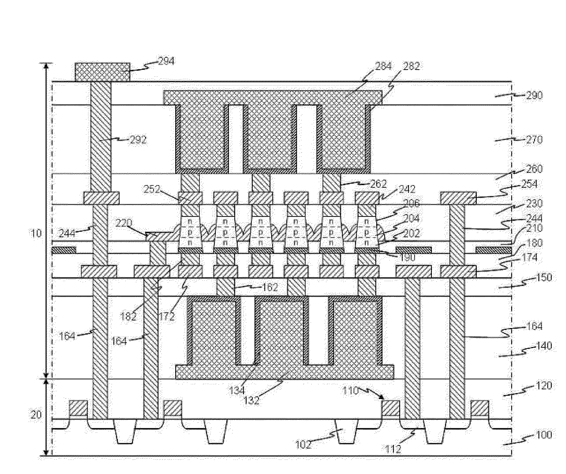
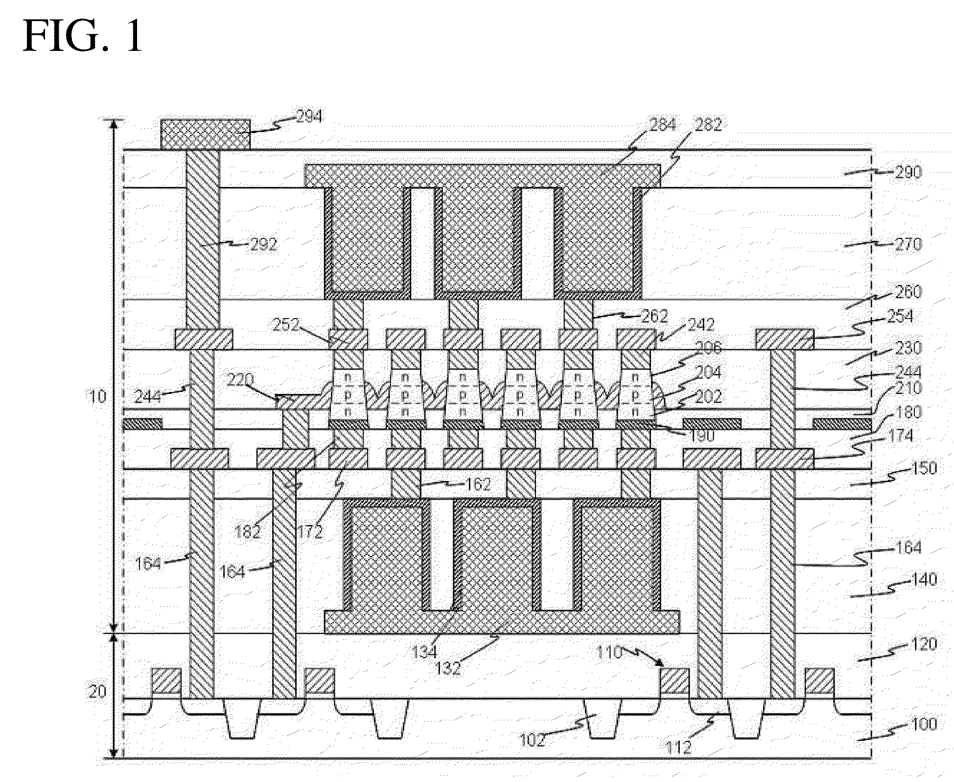
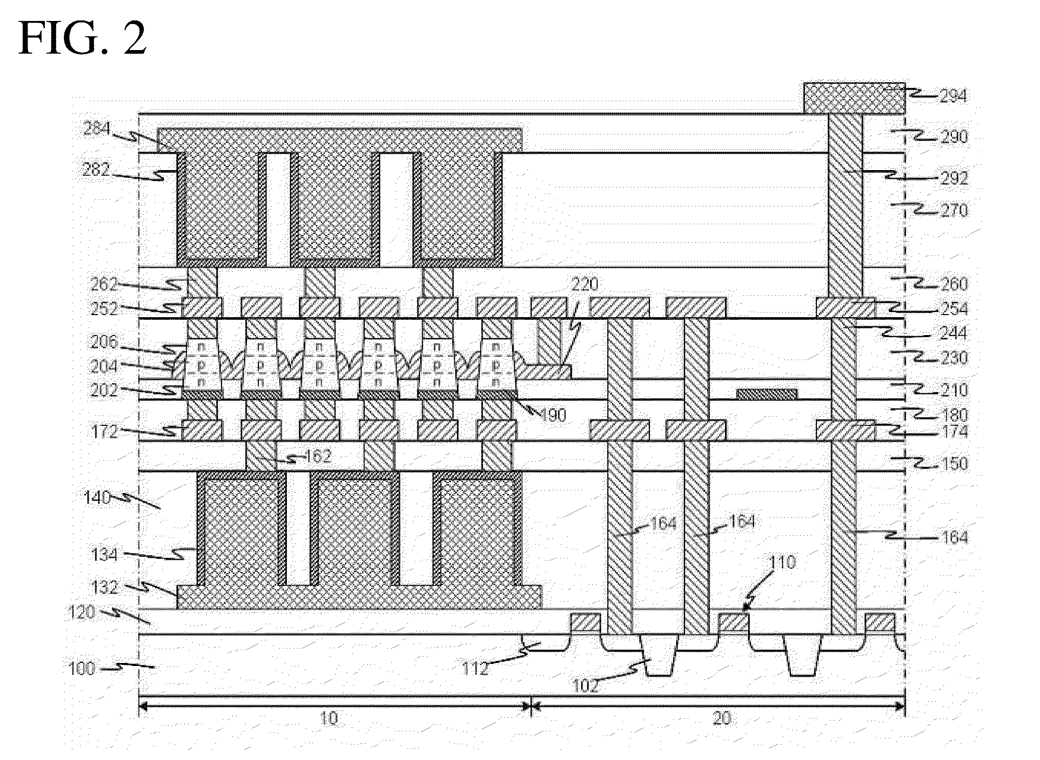
[0043]FIG. 1 is a sectional view of one embodiment of a DRAM device. In this embodiment, the DRAM device includes a logic region 20 and memory cell region 10 which are carried by a semiconductor substrate 100. Specifically, a memory cell region 10 is carried by the logic region20. The logic region 20 on the semiconductor substrate 100 includes logic devices. The memory cell region 10 is spaced apart from the semiconductor substrate 100, and includes switching devices and storage devices. In other embodiments, the logic region can be positioned on the memory cell region 10.

[0044]The semiconductor substrate 100 can include bulk silicon, bulk silicon-germanium, or semiconductor substrate with silicon or silicon-germanium epitaxial layer formed on the substrate. Also, the semiconductor substrate 100 can include silicon-on-sapphire(SOS), silicon-on-insulator(SOI), thin film transistor(TFT), dope or undoped semiconductors, silicon epitaxial layer formed on base semiconductor substrate.

[00...


PUM


Abstract

A method includes forming a switching device which includes a vertical channel spaced apart from a semiconductor substrate, and forming a storage device which is positioned on opposed sides of the switching device. The storage device includes a cylindrically shaped storage node, a plate electrode coupled to the storage node, and a dielectric film which is formed between the storage node and plate electrode, the storage nodes being electrically connected to the switching device.

Description

CROSS-REFERENCE TO RELATED APPLICATIONS[0001]This application claims the benefit of Korean Patent Apps. No. 2008-123595 filed on Dec. 5, 2008, the contents of which are incorporated herein by reference.[0002]This application claims the benefit of Korean Patent Apps 10-2008-0100893 filed on Dec. 5, 2008, the contents of which are incorporated herein by reference.[0003]This application claims the benefit of Korean Patent Application 10-2008-0100892 filed on Dec. 5, 2008, the contents of which are incorporated herein by reference.[0004]This application claims the benefit of Korean Patent Application No. 10-2008-50946, filed on May 30, 2008, the contents of which are incorporated herein by reference.[0005]This application is a continuation-in-part of, and claims the benefit of, U.S. patent application Ser. No. 12 / 470,344, which claims the benefit of Republic of Korea Patent Application No. 10-2008-0046991, the contents of which are incorporated herein by reference.[0006]This application...

Claims


Application Information

Patent Timeline
Patent Type & Authority Patents(United States)
IPC IPC(8): H01L21/00
CPCH01L21/2007H01L21/8221H01L21/823487H01L21/823885H01L24/83H01L27/0688H01L24/29H01L2224/291H01L2224/8385H01L2924/01005H01L2924/01013H01L2924/01015H01L2924/01029H01L2924/01032H01L2924/0104H01L2924/01042H01L2924/0105H01L2924/01073H01L2924/01074H01L2924/01075H01L2924/04941H01L2924/04953H01L2924/07802H01L2924/13091H01L2924/14H01L2924/19041H01L2924/19043H01L2924/30105H01L2224/2919H01L2924/01019H01L2924/01033H01L2924/0665H01L2924/00H01L2924/0132H01L2924/01014H01L2924/3512
Inventor LEE, SANG-YUN
Owner BESANG
Why Eureka
Try Eureka