Production method of a liquid crystal display device including dividing an exposure step into two exposure regions that partly overlap each other and a photomask with a halftone part

a production method and liquid crystal display technology, applied in the direction of liquid crystal compositions, instruments, chemistry apparatus and processes, etc., can solve the problems of substantial inability to irradiate the respective regions for which the exposure is separately performed on the substrate, and the misalignment of about several micrometers at the current technical level, so as to reduce the size of the exposure device, suppress the generation of the joint line on the display screen, and improve the yield

Active Publication Date: 2011-01-18
SHARP KK
View PDF12 Cites 11 Cited by
  • Summary
  • Abstract
  • Description
  • Claims
  • Application Information

AI Technical Summary

Benefits of technology

[0055]According to the production method of the liquid crystal display device of the present invention, generation of the joint line on the display screen is suppressed and the yield can be improved even if the substrate is subjected to the alignment treatment by completing the exposure for the substrate through several exposures in a liquid crystal display device including pixels each having two or more domains. Accordingly, even a large liquid crystal display device in 60-inch model can be stably produced, and the exposure device can be downsized. According to the liquid crystal display device of the present invention, the position and the width of the dark line are continuously changed. Therefore, generation of the joint line on the display screen can be suppressed.

Problems solved by technology

However, it is substantially impossible to irradiate the respective regions for which the exposure is separately performed on the substrate, under completely the same conditions, even if the exposure is performed by an exposure device with the highest accuracy and using a photomask having a pattern with the highest accuracy.
That is, even if the photomask is aligned with the highest accuracy as much as possible on the exposure device, misalignment of about ±several micrometers is inevitable at the current technical level.

Method used


Image

  • Production method of a liquid crystal display device including dividing an exposure step into two exposure regions that partly overlap each other and a photomask with a halftone part
  • Production method of a liquid crystal display device including dividing an exposure step into two exposure regions that partly overlap each other and a photomask with a halftone part
  • Production method of a liquid crystal display device including dividing an exposure step into two exposure regions that partly overlap each other and a photomask with a halftone part

Examples


embodiment 1

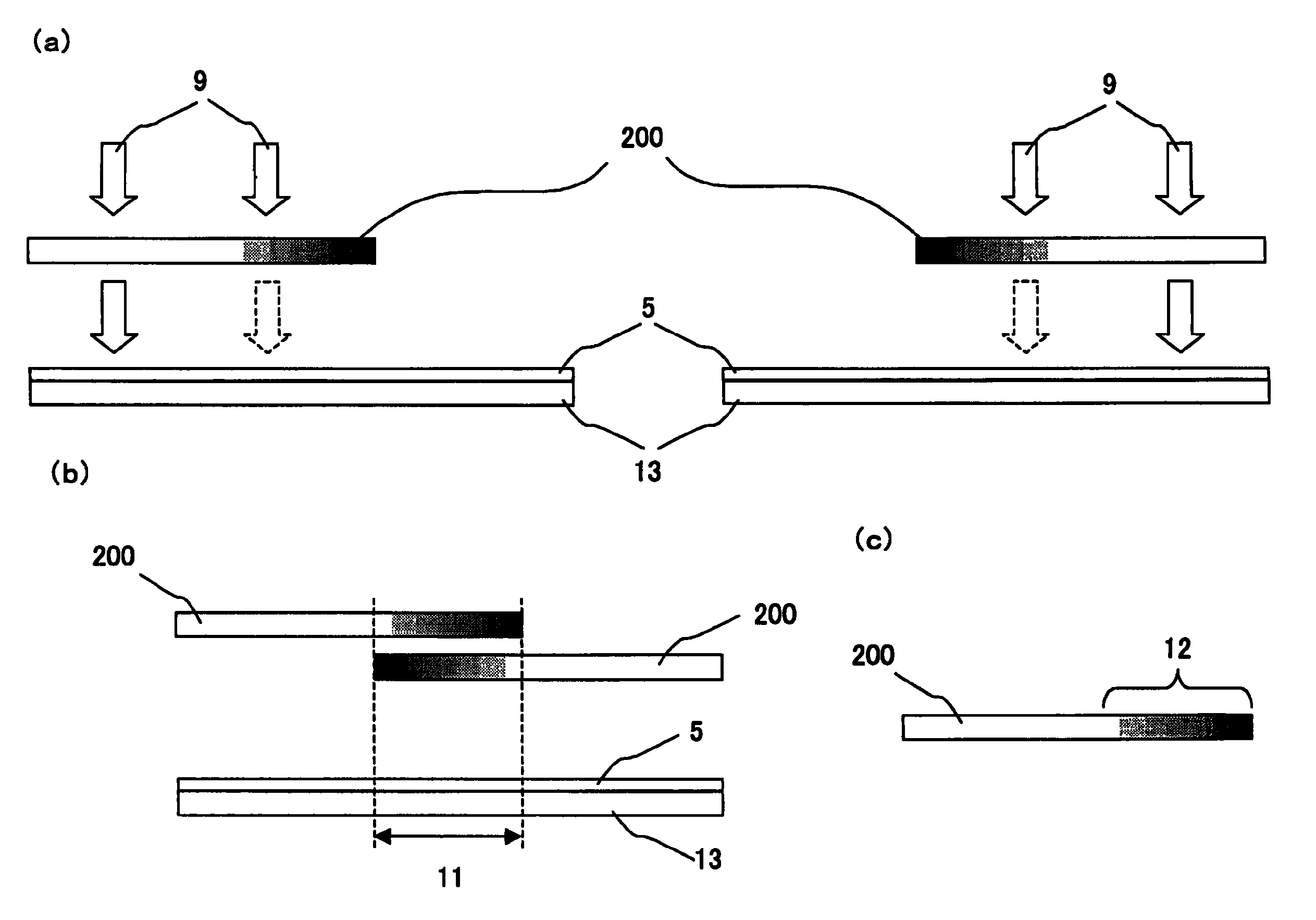
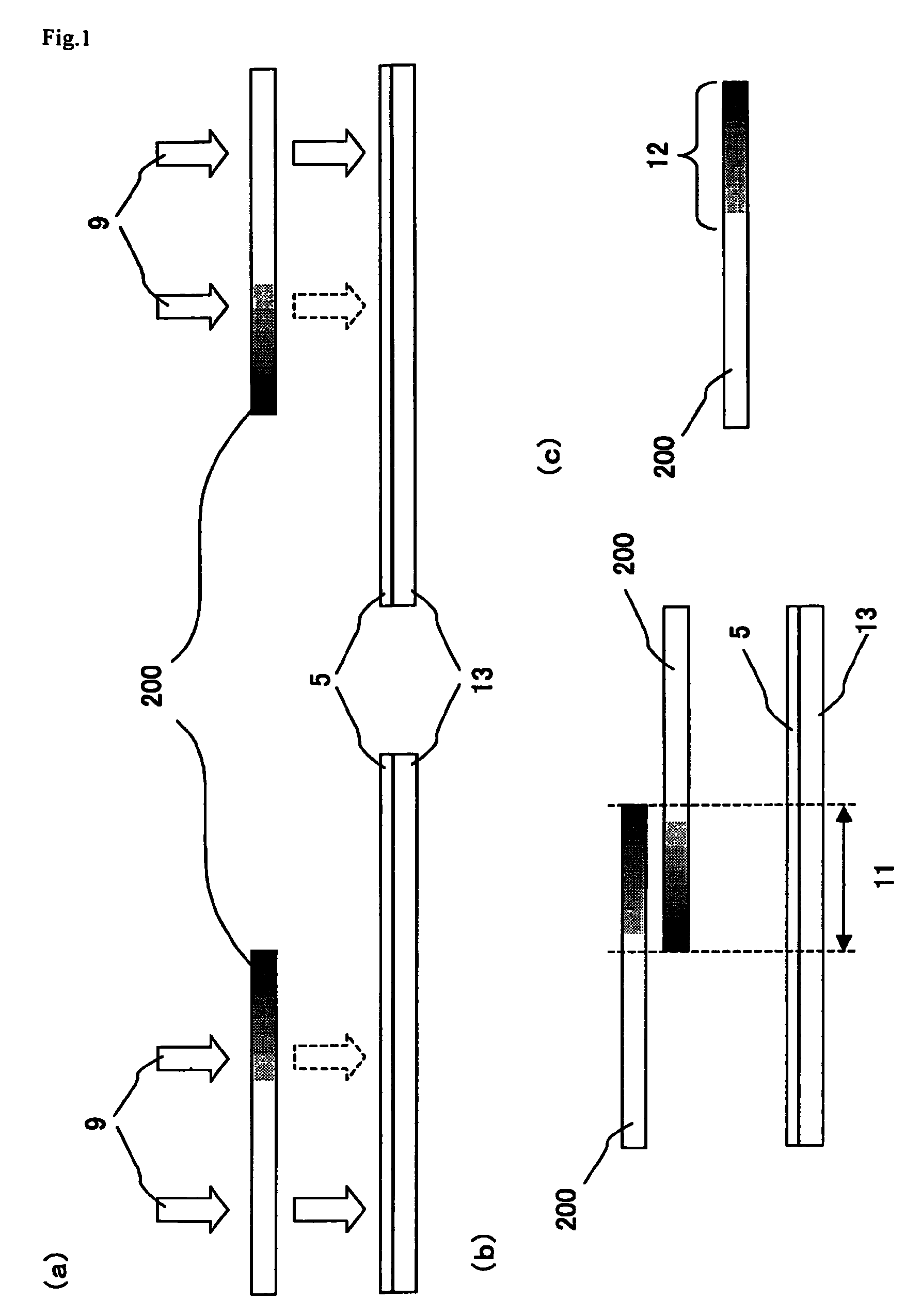
[0128]With regard to a liquid crystal display device in accordance with Embodiment 1 of the present invention, 1. Configuration of liquid crystal display device, 2. Exposure method, 3. Screen joint shot process, 4. Photomask pattern, and 5. Verification test for sample panel are mentioned below.

1. Configuration of Liquid Crystal Display Device

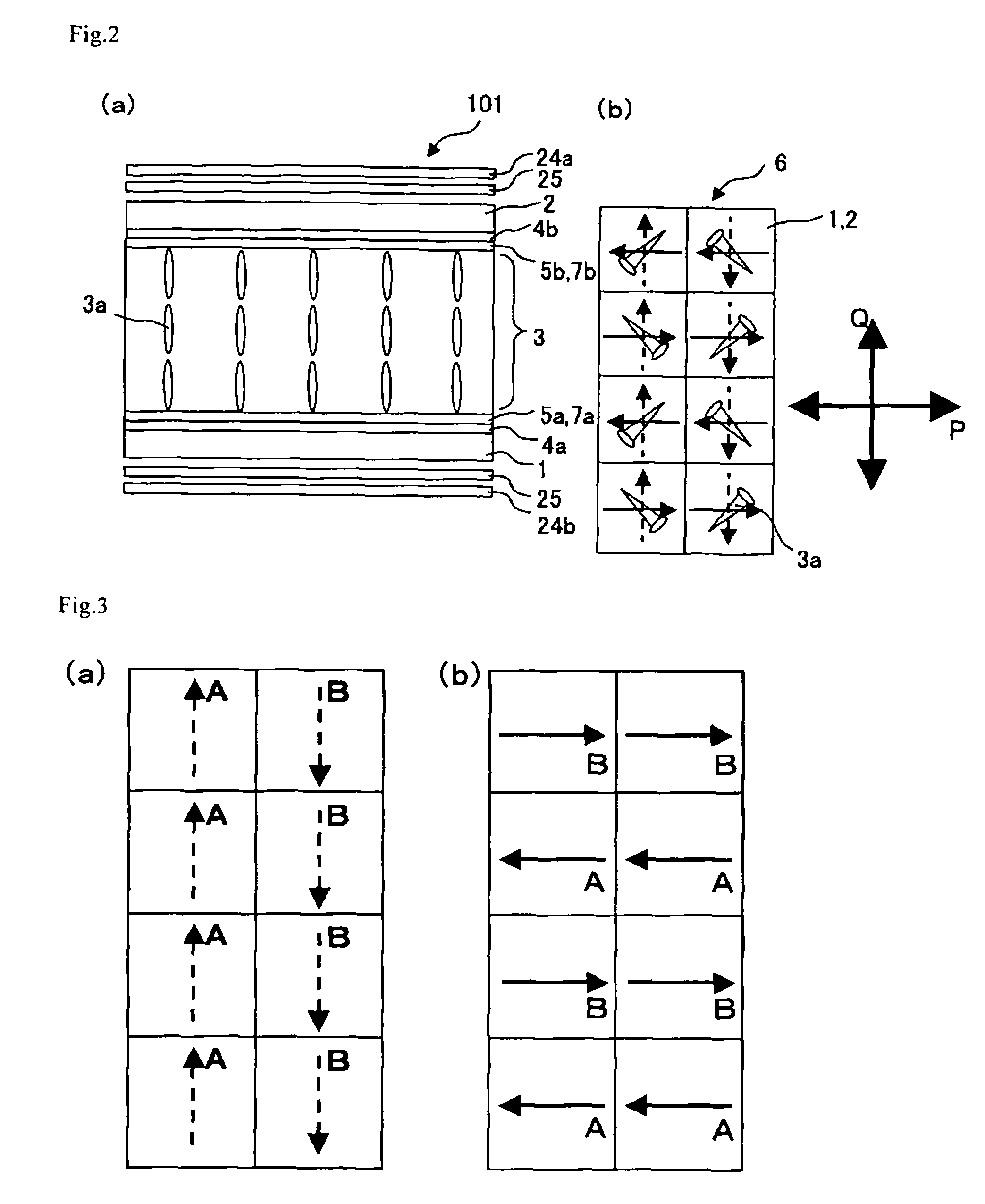
[0129]The configuration of the liquid crystal display device in accordance with Embodiment 1 of the present invention is mentioned, first. The liquid crystal mode of the liquid crystal display device in accordance with the present Embodiment is in four-domain VATN mode.

[0130]FIG. 2(a) is a cross-sectional view showing a configuration of one pixel in the liquid crystal display device in accordance with Embodiment 1. As shown in FIG. 2(a), a liquid crystal display device 101 includes a pair of opposed substrates, i.e., the first substrate 1 (for example, a TFT array substrate) and the second substrate 2 (for example, a CF substrate), and a liquid...

embodiment 2

[0184]A liquid crystal display device in accordance with Embodiment 2 of the present invention is mentioned below.

[0185]FIG. 22 is a schematic view showing a screen joint shot process in accordance with the present Embodiment. As shown in FIG. 22(a), this process adopts scanning exposure in which the light source 15 and the photomask 200 are integrally moved or the substrate 16 is moved with the light source 15 and the photomask 200 being fixed. FIG. 22(a) shows the latter case where the substrate is moved. The substrate 16 is a TFT array substrate. The photomask 200 is equipped with a camera for image detection 17 at its side. The camera scans the bus line 22 on the substrate 16, the BM, and the like, and in accordance with the scanning, the substrate 16 can be moved. This screen joint shot process has an advantage that the exposure device can be downsized; costs on the exposure device are reduced; a photomask having high accuracy can be used because a small one is sufficient. The ...


PUM

PropertyMeasurementUnit
widthaaaaaaaaaa
widthaaaaaaaaaa
widthaaaaaaaaaa

Abstract

To provide a production method of a liquid crystal display device and a liquid crystal display device, in which generation of a joint line on a display screen is suppressed and yield can be improved even if a substrate is subjected to an alignment treatment by completing exposure for the substrate through several exposures in a liquid crystal display device including pixels each having two or more domains. The present invention is a production method of a production method of a liquid crystal display device, the liquid crystal display device including: a pair of opposed substrates; a liquid crystal layer formed between the pair of opposed substrates; and an alignment film arranged on a liquid crystal layer side surface of at least one of the pair of opposed substrates, and the liquid crystal display device having two or more regions which differ in alignment azimuth in a pixel, wherein the production method comprises an exposure step of exposing the alignment film in such a way that a substrate plane is divided into two or more exposure regions through a photomask in each exposure region, and in the exposure step, exposure is performed in such a way that adjacent two exposure regions have an overlapping exposure region where the adjacent two exposure regions partly overlap with each other, and the photomask has a halftone part corresponding to the overlapping exposure region.

Description

[0001]This application is the U.S. national phase of International Application No. PCT / JP2007 / 051192, filed 25 Jan. 2007, which designated the U.S. and claims priority to Japan Application No. 2006-017755, filed 26 Jan. 2006, the entire contents of each of which are hereby incorporated by reference.TECHNICAL FIELD[0002]The present invention relates to a method for producing a liquid crystal display device and a liquid crystal display device. More specifically, the present invention relates to a method for producing a matrix liquid crystal display device and a matrix liquid crystal display device, in which high display qualities can be obtained by forming two or more domains in a pixel.BACKGROUND ART[0003]A liquid crystal display device has been widely used in a TV, a monitor for personal computers, and the like, because it is a display device with low power consumption and it can be reduced in weight and thickness. However, according to the liquid crystal display device, light polar...

Claims


Application Information

Patent Timeline
Patent Type & Authority Patents(United States)
IPC IPC(8): G02F1/1337
CPCG02F1/133788G02F1/133753
Inventor INOUE, IICHIROHAKOI, HIROYUKITERASHITA, SHINICHIMIYACHI, KOICHI
Owner SHARP KK
Why Eureka
Try Eureka