Tunable embedded inductor devices

a high-frequency inductor and inductor technology, applied in the direction of transformer/inductance details, printed inductances, basic electric elements, etc., can solve the problems of affecting the entire circuit, increasing processing period and fabrication costs, and formation of electric conductive shorting members that are not suitable for regulating high-frequency inductor devices embedded in functional substrates

Active Publication Date: 2011-02-08
IND TECH RES INST
View PDF11 Cites 143 Cited by
  • Summary
  • Abstract
  • Description
  • Claims
  • Application Information

AI Technical Summary

Problems solved by technology

During development and design of high frequency circuit modules, consideration must be given to inductor devices, as they are electrically coupled to other peripheral circuits or devices and may be vulnerably interfered with thereof.
Additionally, the inductor devices can be affected by process and material variations such that characteristics of the inductor devices are not precise, resulting in detrimental performance of the entire circuitry.
Each time the circuit layout design is changed, the high frequency circuit module testing boards are also remade, thereby increasing processing period and fabrication costs.
However, formation of the electric conductive shorting member is not suitable for regulating high frequency inductor device embedded in functional substrates.
Conventional planar wound inductor devices can not be integrated into multi-layered inductor structures.
More specifically, when a passivation layer or an outer substrate is formed on the planar wound inductor device, it is difficult to precisely trim segments of the planar spiral coil.

Method used


Image

  • Tunable embedded inductor devices
  • Tunable embedded inductor devices
  • Tunable embedded inductor devices

Examples


Embodiment Construction

[0026]It is to be understood that the following disclosure provides many different embodiments, or examples, for implementing different features of various embodiments. Specific examples of components and arrangements are described below to simplify the present disclosure. These are merely examples and are not intended to be limiting. In addition, the present disclosure may repeat reference numerals and / or letters in the various examples. This repetition is for the purpose of simplicity and clarity and does not in itself indicate a relationship between the various embodiments and / or configurations discussed. Moreover, the formation of a first feature over or on a second feature in the description that follows may include embodiments in which the first and second features are formed in direct contact or not in direct contact.

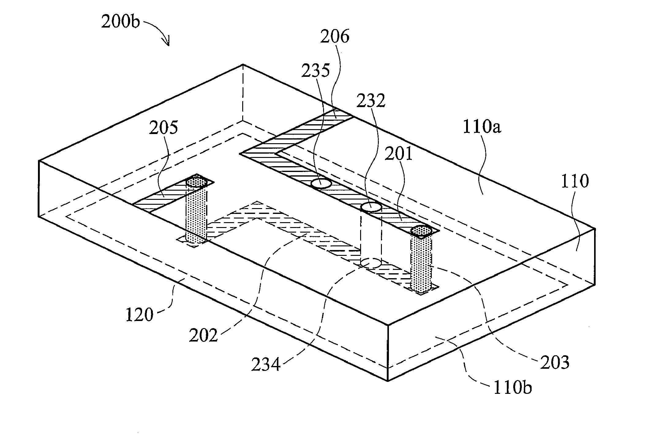
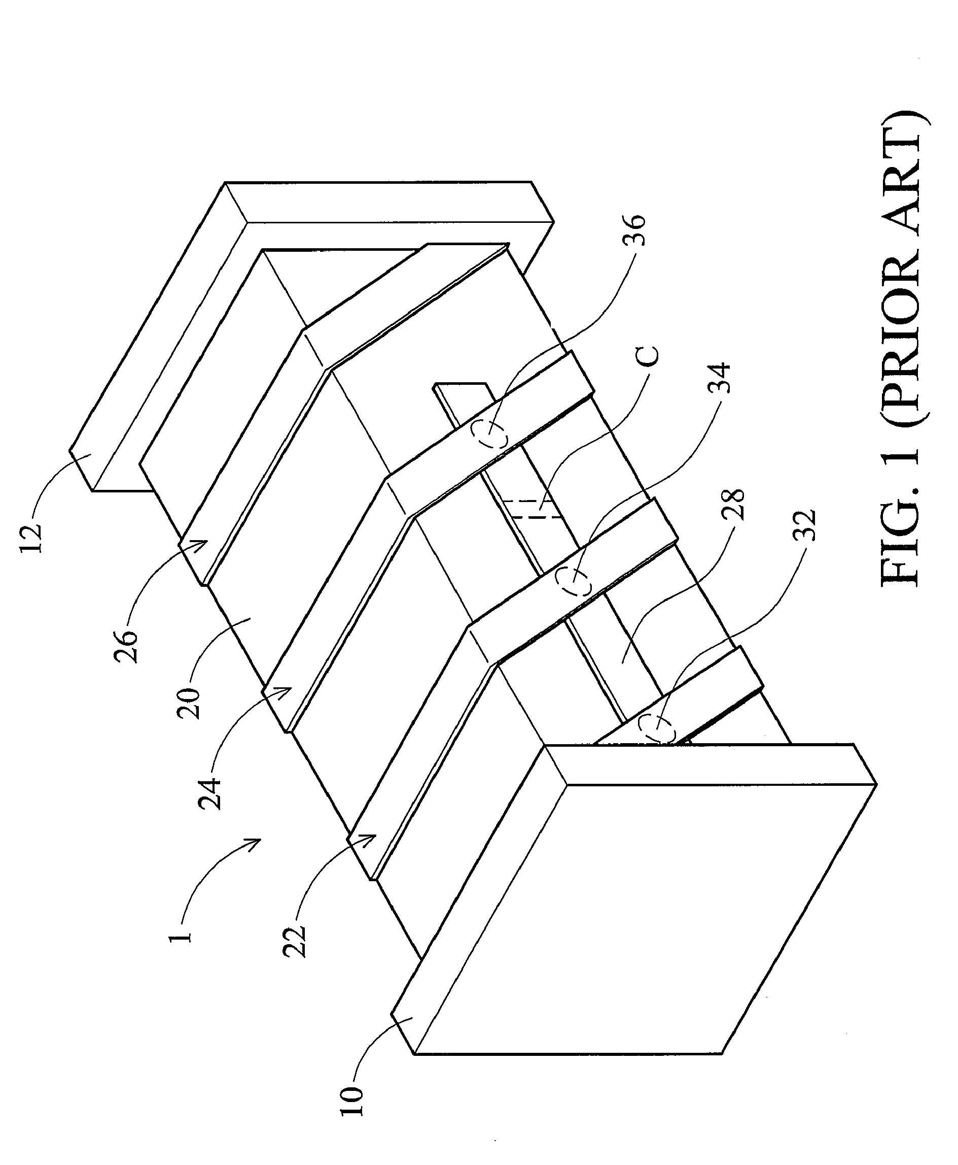
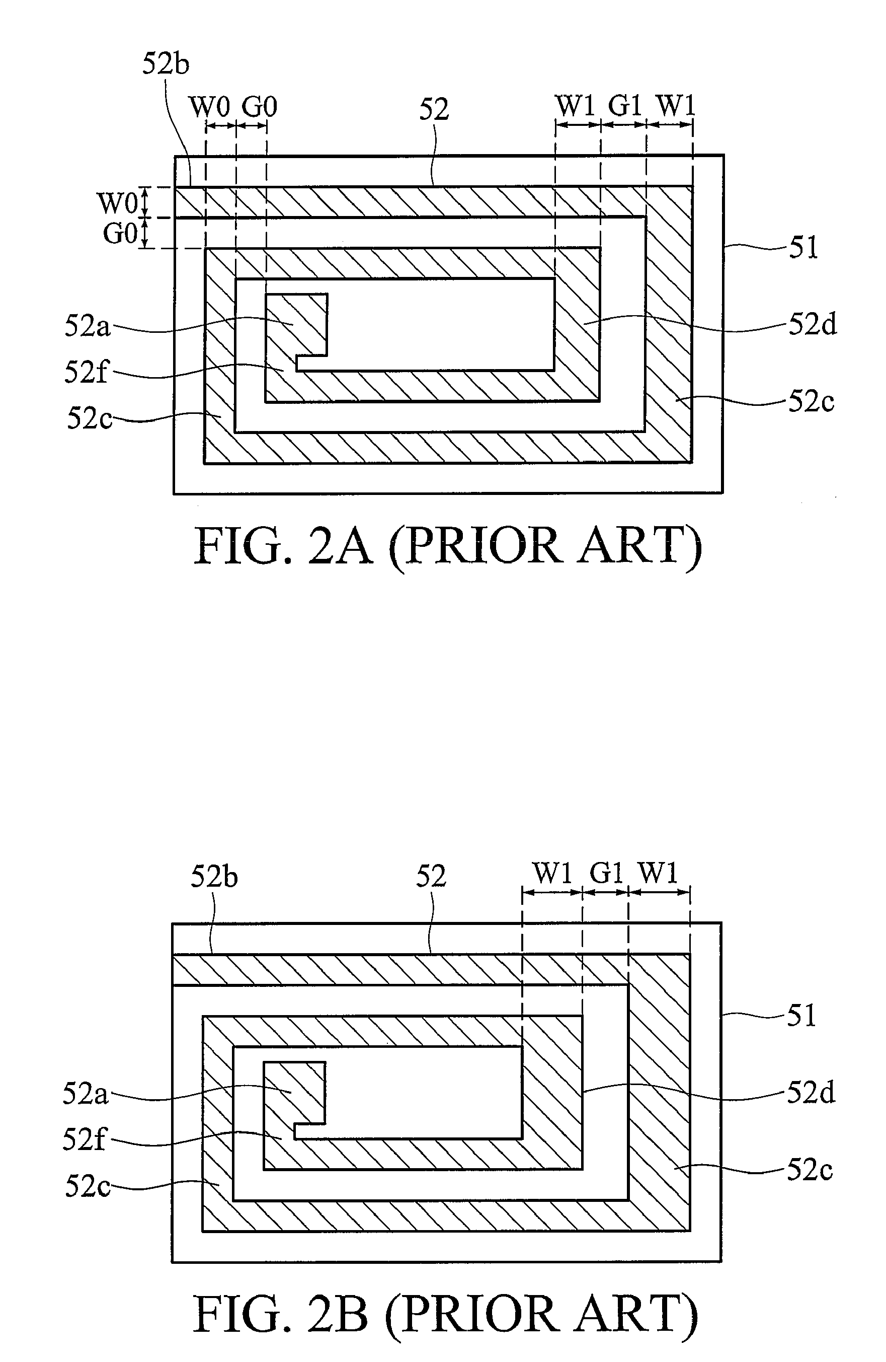
[0027]As mentioned previously, during development and design of high frequency circuit modules, consideration must be given to inductor devices, as they are elec...


PUM

PropertyMeasurementUnit
inductanceaaaaaaaaaa

Abstract

The invention provides tunable embedded high frequency inductor devices. The inductor device comprises a dielectric substrate. A first conductive line is disposed on a first surface of the dielectric substrate. A second conductive line is disposed on a second surface of the dielectric substrate. An interconnection is disposed perforating the dielectric substrate and connecting the first conductive line with the second conductive line. A coupling region is defined between the first and the second conductive lines. A conductive plug connecting the first conductive line and the second line is disposed in the coupling region. Alternatively, an opening is disposed in the first and second conductive lines to tune inductance of the inductor.

Description

BACKGROUND OF THE INVENTION[0001]1. Field of the Invention[0002]The invention relates to tunable embedded inductor devices, and in particular to tunable embedded high frequency integrated inductor devices.[0003]2. Description of the Related Art[0004]Embedded inductor devices have been applied in various circuits including resonators, filters, and matching networks. Among applications of wireless communication, digital computer, portable electronics, and information household appliance, features with higher frequencies, broader bandwidths, and miniaturization have become main requirements of high-tech industries and commercial markets. During development and design of high frequency circuit modules, consideration must be given to inductor devices, as they are electrically coupled to other peripheral circuits or devices and may be vulnerably interfered with thereof. Additionally, the inductor devices can be affected by process and material variations such that characteristics of the i...

Claims


Application Information

Patent Timeline
Patent Type & Authority Patents(United States)
IPC IPC(8): H01F5/00
CPCH01F21/12H01F17/0006H01F41/045H01F2017/002H01F2021/125
Inventor WEI, CHANG-LINTSAI, CHENG-HUASHYU, CHIN-SUNCHIN, KUO-CHIANGYU, SYUN
Owner IND TECH RES INST
Why Eureka
Try Eureka