Power semiconductor device

a technology of semiconductor devices and semiconductors, applied in the direction of semiconductor devices, basic electric elements, electrical equipment, etc., can solve the problems of adversely affecting the leakage current of gate electrodes and the primary voltage-to-leakage-current characteristics, and achieve the effect of reducing the reducing the gate resistance of gate electrodes, and improving the imbalance of current diversions at turn-o

Active Publication Date: 2011-02-15
SONRAI MEMORY LTD
View PDF19 Cites 14 Cited by
  • Summary
  • Abstract
  • Description
  • Claims
  • Application Information

AI Technical Summary

Benefits of technology

[0016]The present invention is aimed to solve the problems above-described; an object thereof is, even when the spaces between the gate wiring 53 become wide, to provide a power semiconductor device that can meet requirements for larger current capacity and higher reliability while improving imbalance among current diversions.
[0018]According to the present invention, because a power semiconductor device is configured so as to have a gate electrode including a polysilicon film provided on a gate insulation film, and a doped polysilicon film—a polysilicon doped with impurities to reduce its resistance—that is provided on the polysilicon film; the gate resistance of the gate electrode can be reduced in comparison to conventional ones. Therefore, the imbalance among current diversions at turn-off is improved so as not to reduce turn-off withstand ability of the device. In addition, because a polysilicon film not doped with impurities is provided between a doped polysilicon film and a gate insulation film, it is possible to preclude auto-doping of impurities, which might be feared by providing with the doped polysilicon film, into the gate insulation film and an n− layer from adversely affecting gate-emitter leakage current and collector-emitter leakage current. Therefore, a power semiconductor device that meets requirements for increased current capacity and higher reliability can be obtained.

Problems solved by technology

However, when doped silicon is used for the gate electrode 61 of the planar-gate-type IGBT shown in FIG. 8 and FIG. 9, auto-doping of impurities, with which a polysilicon has been doped, into the gate insulation film 60 and the n− layer 57 occurs, adversely affecting the gate-emitter leakage current and the primary-voltage-to-leakage-current characteristics.

Method used


Image

  • Power semiconductor device
  • Power semiconductor device
  • Power semiconductor device

Examples


embodiment 1

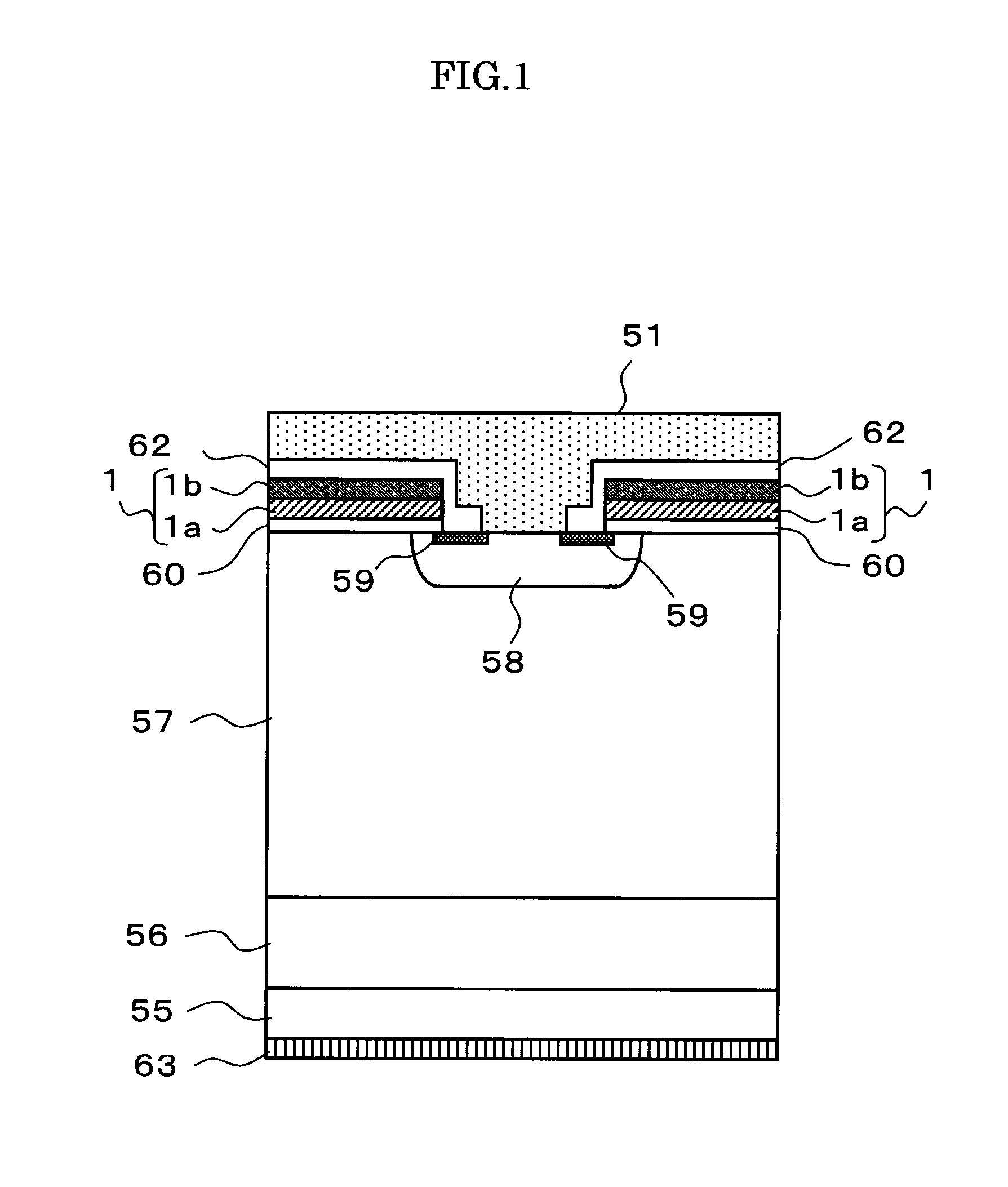
[0029]Embodiment 1 according to the present invention will be explained below. FIG. 1 is a partial cross-sectional view illustrating a planar-gate-type IGBT that is a power semiconductor device according to Embodiment 1 of the present invention; the figure illustrates, taking along the line A-A, a cross-sectional cellar structure of the IGBT cells 54 shown in FIG. 7. FIG. 1 differs from FIG. 8 that represents prior art as follows; a gate electrode includes a polysilicon film 1a provided on the gate insulation film 60, and a doped polysilicon film 1b that is doped with impurities and provided on the polysilicon film 1a; the gate electrode 1 is connected to the gate wiring 53 at the electrode ends provided in its extension orientation (in the front-back orientation with respect to the document face in FIG. 1). Because the other components are identical or equivalent to those in FIG. 8, the same numerals will be used so as to omit their explanations.

[0030]According to the structure sho...

embodiment 2

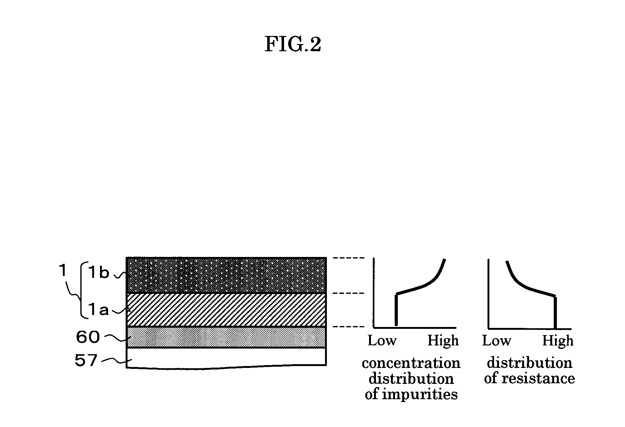
[0033]In Embodiment 1, a gate electrode 1 has been explained, in which the gate electrode 1 is configured with the polysilicon film 1a provided on the gate insulation film 60, and the doped polysilicon film 1b that is doped with impurities to reduce its resistance and is provided on the polysilicon film 1a. One of FIG. 2 is a partially enlarged view for explaining Embodiment 2; the figure corresponds to a view in which the gate electrode 1 in FIG. 1 is partially enlarged. Embodiment 2 differs from Embodiment 1 in that gradient of concentration with respect to impurities is provided in the doped polysilicon film 1b. More specifically, as distribution of its impurity concentration shown in the middle view of FIG. 2, the impurity concentration is made to vary in a thickness direction of the doped polysilicon film 1b; at the top portion of the doped polysilicon 1b, the value of impurity concentration takes its maximum value; the value becomes smaller heading thickness-wise toward the po...

embodiment 3

[0037]The gate electrode 1 configured with a polysilicon film 1a and a doped polysilicon 1b that have been explained in Embodiment 1, is also applicable to a planar-gate-type IGBT that has a terrace gate structure shown in FIG. 9. FIG. 3 is a partial cross-sectional view illustrating a planar-gate-type IGBT that is a power semiconductor device having the terrace gate structure, according to Embodiment 3 of the present invention; the figure illustrates, taking along the line A-A, a cellar structure of the IGBT cells 54 shown in FIG. 7. FIG. 3 differs from FIG. 9 explaining a conventional device, as follows; a terrace gate portion 65 of a gate electrode 2 is configured with a polysilicon film 2a provided on a gate insulation film 60, and with the doped polysilicon film 2b that is provided on the polysilicon film 2a and is doped with impurities to reduce its resistance. In addition, the gate electrode 2 is connected to the gate wiring 53 at the electrode ends provided in its extension ...


PUM


Abstract

A power semiconductor having a first, second, third, and fourth semiconductor layer on top of each other, two trench gates parallel and adjacent to each other, each having a trench in the fourth semiconductor layer with the a trench bottom portion reaching into the third semiconductor layer, a gate insulation film lining the trench, and a gate electrode filling the trench being lined with the gate insulation film, two first semiconductor region regions provided contiguously bordering on one side of each of the two trench gates, located at the outer sides of each of the two adjacent trench gates, and located in the top side of the fourth semiconductor layer, a first main electrode on the fourth semiconductor layer, and a second main electrode provided on a bottom of the first semiconductor layer.

Description

BACKGROUND OF THE INVENTION[0001]1. Field of the Invention[0002]The present invention relates to power semiconductor devices having a MOS-gate-metal-oxide semiconductor gate-structure, especially to an insulated gate bipolar transistor used in devices such as invertors that transform or control electric power.[0003]2. Description of the Related Art[0004]In recent years, insulated gate bipolar transistors (hereinafter referred as IGBTs) are utilized, in many cases, as power semiconductor devices including invertors that transform or control electric power. Also, IGBTs are required to obtain larger current capacity (higher withstand voltage) and higher reliability.[0005]FIG. 7 is a plane view of an IGBT-chip that is illustrated in Patent Document 1, for example. In the IGBT-chip 50 illustrated in FIG. 7, a numeral ‘51’ represents an emitter electrode (a first main electrode); ‘52’, a gate pad formed at a concave portion that is provided on a peripheral portion of the emitter electrode...

Claims


Application Information

Patent Timeline
Patent Type & Authority Patents(United States)
IPC IPC(8): H01L29/739
CPCH01L29/0696H01L29/0847H01L29/7397H01L29/4236H01L29/4916H01L29/7395H01L29/407H01L29/42368
Inventor SUEKAWA, EISUKE
Owner SONRAI MEMORY LTD
Why Eureka
Try Eureka