Supercharge Your Innovation With Domain-Expert AI Agents!

System in package integrating a plurality of semiconductor chips

a technology of semiconductor chips and components, applied in the field of system in packages, can solve the problems of reducing the percentage of non-defective items, low manufacturing process efficiency, and the inability to implement the kind of functional blocks by the process, so as to shorten the time required for the manufacturing process and achieve low development cost. , the effect of simple process

Active Publication Date: 2011-02-15
RENESAS ELECTRONICS CORP
View PDF15 Cites 7 Cited by
  • Summary
  • Abstract
  • Description
  • Claims
  • Application Information

AI Technical Summary

Benefits of technology

The present invention provides a system in package that integrates multiple semiconductor chips. The first chip is a common component in multiple system in packages and includes a central processing unit. The second chip has different specifications for each system in package and includes a module substrate with the first chip. The first chip has a module connection terminal and the second chip has a corresponding module connection terminal connected by a bonding wire. This design allows for the creation of customized products with individual functions in addition to common functions in a short period of time. The use of the system in package simplifies the manufacturing process and reduces development costs.

Problems solved by technology

However, some kind of functional blocks cannot be implemented by the process or have low efficiency in manufacturing the process.
For example, if a chip size is too large due to the need for mounting a high-capacity memory or the like, the percentage of non-defective items decreases significantly to fail to manufacture a semiconductor chip.
Thus, the use of a SoC tales a long development period and requires a high development cost.
Further, because a SiP allows connection of different chips, a limitation on chip size is significantly less than a SoC.
The redesign leads to a longer development period and a higher development cost.

Method used


Image

  • System in package integrating a plurality of semiconductor chips
  • System in package integrating a plurality of semiconductor chips
  • System in package integrating a plurality of semiconductor chips

Examples


first embodiment

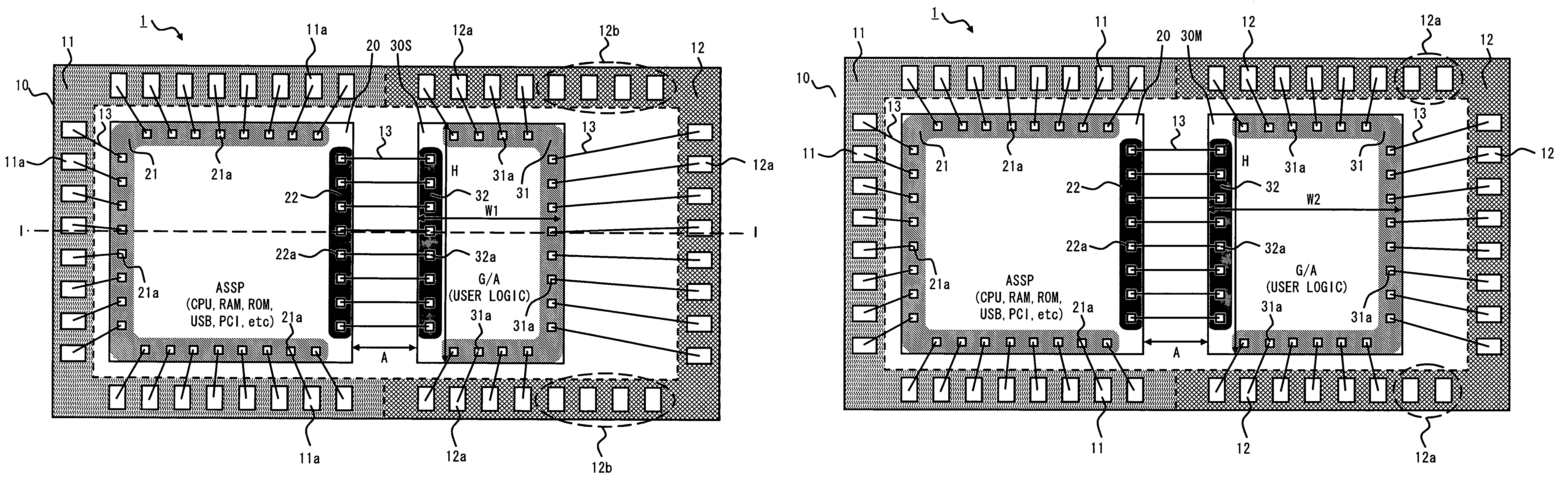
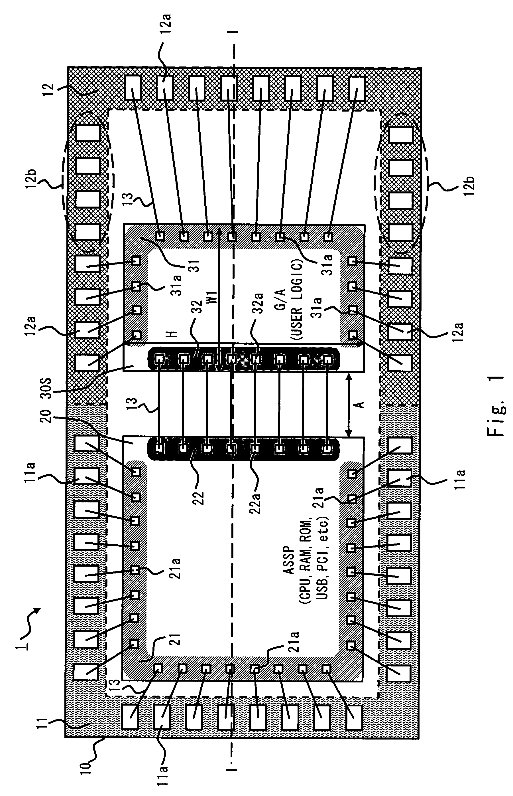
[0027]Exemplary embodiments of the present invention are described hereinafter with reference to the drawings. In the following description, not every one of a group of elements such as pads and bonding wires is denoted by a reference numeral for simplification of the drawings. The elements having the same shape located in the same area as the element denoted by a reference numeral are the same as the denoted element. FIG. 1 is a plan view of a semiconductor apparatus according to a first embodiment of the present invention. The semiconductor apparatus of this embodiment is a System in Package (which is referred to hereinafter simply as a SiP) that integrates a system including a CPU into one package. As shown in FIG. 1, a SiP 1 of this embodiment includes a module substrate 10, a first chip (e.g. Application Specific Standard Product (ASSP)) 20, a second chip (e.g. Gate Array (G / A)) 30S, for example.

[0028]The module substrate 10 includes module pads 11a, 12a and 12b in its peripher...

second embodiment

[0050]A SiP 2 according to a second embodiment of the present invention is such that an ASSP that is used in common among different SiPs 2 is a semiconductor apparatus of a BGA type. FIG. 9 shows a plan view of the SiP 2. As shown in FIG. 9, in the SiP 2, an ASSP 50, which is a semiconductor apparatus that is equivalent to the ASSP 20 of the first embodiment, is mounted on a module substrate 40. On the module substrate 40, first module connection terminals 42 are placed along the side of the ASSP 50 that faces the G / A 30S. The first module connection terminals 42 are connected with prescribed terminals of the ASSP 50 by inter-substrate lines of wiring layers formed inside the module substrate. In the second embodiment also, the second module connection terminals 32a of the G / A 30S are connected with the first module connection terminals 42 by the bonding wires 13.

[0051]FIG. 10 shows a plan view where the ASSP 50 is removed from the module substrate 40 of the SiP 2. As shown in FIG. ...

third embodiment

[0053]The SiP 1 according to the first embodiment includes BGA-type terminals. On the other hand, a SiP 3 according to a third embodiment of the invention includes pin-type terminals. FIG. 12 shows a plan view of the SiP 3. As shown in FIG. 12, the ASSP 20 and the G / A 30S are connected by the bonding wire 13 in the SiP 3 as well. The ASSP 20 and the G / A 30S are mounted on an inner lead 63. Module terminals 61 are placed in the periphery of a lead frame as terminals that are equivalent to the module pads placed in the common pad placement area 11. Further, module terminals 62 and 62a are placed as terminals that are equivalent to the module pads placed in the individual pad placement area 12. The module terminals 61 and 62 are connected with the chip pads 21a of the ASSP 20 and the chip pads 31a of the G / A 30S, respectively, by the bonding wires 13. In the SiP 3, the module terminals 61 correspond to the first module terminals 14a of the first embodiment, and the module terminals 62 ...


PUM


Abstract

A system in package integrating a plurality of semiconductor chips, including a first chip mounted commonly in a plurality of system in packages and at least including a CPU, a second chip having a different specification for each of the plurality of system in packages depending on a connection of internal lines, and a module substrate including the first chip and the second chip adjacent to each other and having a shape common to the plurality of system in packages. The first chip includes a first module connection terminal on the first chip along a first side facing the second chip or in an area different from the first chip and facing the second chip. A second side of the second chip includes a second module connection terminal to be connected with the first chip. The first and the second module connection terminals are connected by a bonding wire.

Description

BACKGROUND OF THE INVENTION[0001]1. Field of the Invention[0002]The present invention relates to a system in package and particularly to a system in package that integrates a chip including a Central Processing Unit (CPU) used in common for a plurality of products and a custom chip including a different wiring layer for each user to implement different specifications into one package.[0003]2. Description of Related Art[0004]Recent semiconductor apparatus integrate the maximum number of functional blocks constituting a system in order to implement many functions with a small mounting area. One of such semiconductor apparatus is a System on Chip (SoC) in which a plurality of functional blocks are formed on a single semiconductor chip. A SoC implements all functional blocks in one semiconductor process. However, some kind of functional blocks cannot be implemented by the process or have low efficiency in manufacturing the process. For example, if a chip size is too large due to the nee...

Claims


Application Information

Patent Timeline
Patent Type & Authority Patents(United States)
IPC IPC(8): H01L23/48H01L23/52H01L29/40
CPCH01L24/49H01L25/0655H01L25/18H01L2224/48091H01L2224/48137H01L2224/48227H01L2224/48247H01L2224/49171H01L2224/49175H01L2924/01082H01L2924/00014H01L2924/01006H01L2924/01033H01L2924/01075H01L2924/014H01L2924/00H01L24/48H01L2224/05554H01L2924/181H01L2224/45099H01L2224/05599H01L2924/00012
Inventor SUZUKI, KATSUNOBUIWASAKI, JUNICHI
Owner RENESAS ELECTRONICS CORP
Features
  • R&D
  • Intellectual Property
  • Life Sciences
  • Materials
  • Tech Scout
  • Unparalleled Data Quality
  • Higher Quality Content
  • 60% Fewer Hallucinations
Learn More