Mode transition between a planar line and a waveguide with a low loss RF substrate and a high loss low frequency substrate

a low-loss, waveguide-type technology, applied in the direction of impedence networks, electrical devices, coupling devices, etc., can solve the problems of inability to miniaturize the mode transition circuit, inability to minimize the micro-strip line, and inability to achieve signal loss, so as to reduce the manufacturing cost of the signal and minimize the loss. , the effect of inexpensive material

Active Publication Date: 2011-03-22
ELECTRONICS & TELECOMM RES INST
View PDF11 Cites 18 Cited by
  • Summary
  • Abstract
  • Description
  • Claims
  • Application Information

AI Technical Summary

Benefits of technology

[0010]In the present invention, a waveguide is formed for integrating a radio frequency (RF) substrate and a low frequency substrate. Therefore, the signal loss generated while transferring a RF signal can be minimized according to the present invention.
[0011]According to the present invention, a baseband processor or a power IC of a low frequency substrate can be effectively integrated with a RF substrate. Therefore, a transceiver module can be miniaturized, and the manufacturing cost thereof can be reduced.
[0012]According to the present invention, a mode transition circuit and a transceiver module using the same can be formed of inexpensive material and simple manufacturing processes.

Problems solved by technology

Since the micro-strip line must include a conductive element such as a back-short, the micro-strip line is not proper in a view of miniaturizing a mode transition circuit.
However, a transmission line such as micro-strip line is still required to connect active elements and a mode transition circuit so the signal loss is unescapable due to the transmission line.
However, the conventional technology of U.S. Pat. No. 5,982,250 still has a shortcoming of a high manufacturing cost and a difficulty of integration if it is integrated with circuits operated in a low frequency circuit, such as a baseband processor or a power integration chip (IC).
However, FR4 has a great substrate loss, and it is not easy to form a RF module using FR4.

Method used


Image

  • Mode transition between a planar line and a waveguide with a low loss RF substrate and a high loss low frequency substrate
  • Mode transition between a planar line and a waveguide with a low loss RF substrate and a high loss low frequency substrate
  • Mode transition between a planar line and a waveguide with a low loss RF substrate and a high loss low frequency substrate

Examples


Embodiment Construction

[0018]Other objects and aspects of the invention will become apparent from the following description of the embodiments with reference to the accompanying drawings, which is set forth hereinafter.

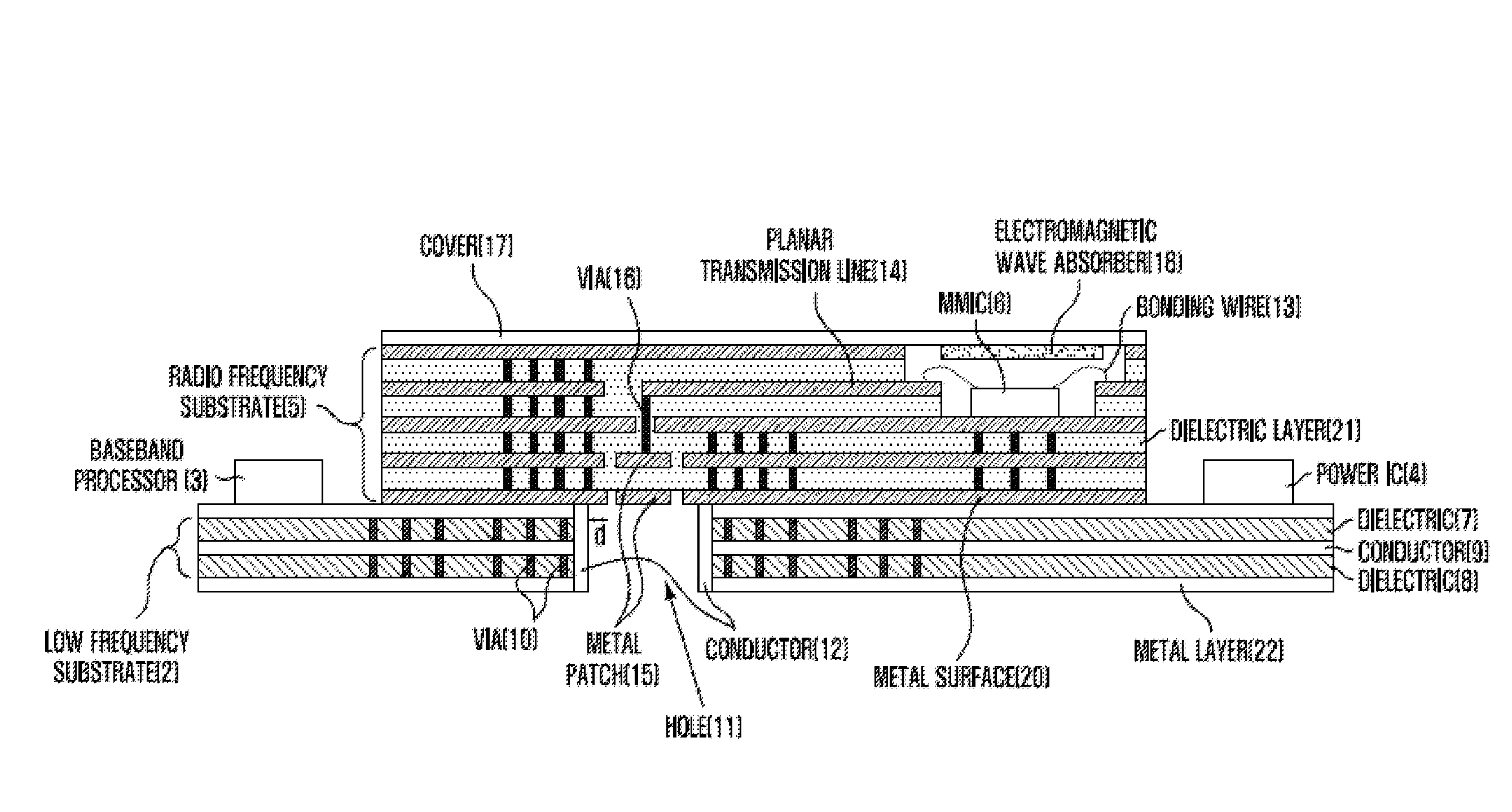
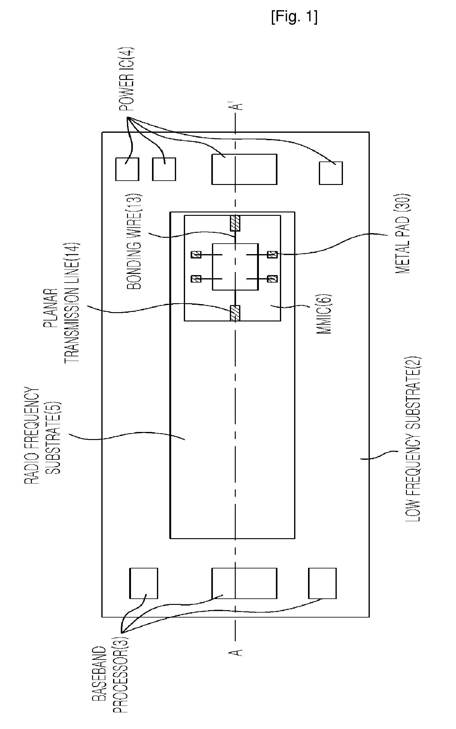
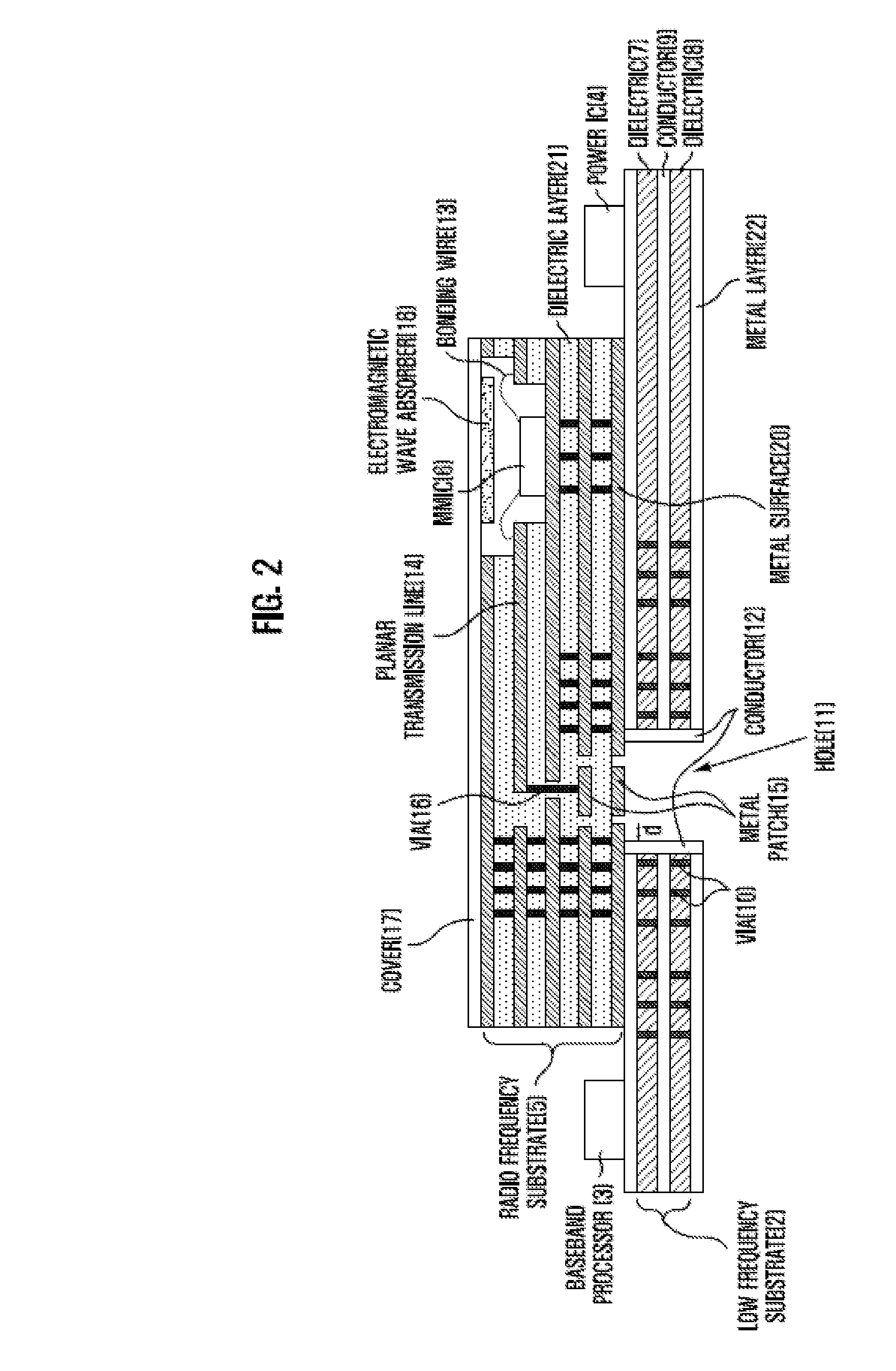
[0019]FIG. 1 is a top view illustrating a transition circuit for transferring a RF signal in accordance with an embodiment of the present invention, FIG. 2 is a cross-sectional view of FIG. 1 taken along the line A-A′ shown in FIG. 1, and FIG. 3 is a bottom view of FIG. 1.

[0020]The present invention proposes a mode transition circuit for transferring a Radio Frequency (RF) signal generated from a RF substrate 5 (FIGS. 1, 2) to a module such as an antenna through a planar transmission line 14 (FIG. 2) and a waveguide including vias 16 (FIG. 2) and metal patches 15 (FIGS. 2, 3) formed inside the RF substrate 5 and a hole 11 (FIG. 2) formed inside a low frequency substrate 2, and a transceiver module having the same.

[0021]As described above, the present invention proposes the mode transition c...


PUM

PropertyMeasurementUnit
radio frequencyaaaaaaaaaa
dielectric constantaaaaaaaaaa
frequencyaaaaaaaaaa

Abstract

Provided is a mode transition circuit for transferring a RF signal and a transceiver module having the same. The mode transition circuit includes: a planar transmission line mounted at a RF substrate for receiving a RF signal from a RF signal generating unit; a via formed inside the RF substrate and connected to one side of the planar transmission line for receiving the RF signal from the planar transmission line; at least one of metal patches formed inside the RF substrate and connected to the one side of the via for receiving the RF signal from the via; and a hole formed inside a low frequency substrate and connected to one side of the metal patch for receiving the RF signal from the metal patch.

Description

TECHNICAL FIELD[0001]The present invention relates to a mode transition circuit for transferring a radio frequency (RF) signal and a transceiver module having the same; and more particularly, to a mode transition circuit for transferring a Radio Frequency signal generated from a RF substrate to a module such as an antenna through a planar transmission line and a waveguide including vias and metal patches formed inside the RF substrate and a hole formed inside a low frequency substrate, and a transceiver module having the same.BACKGROUND ART[0002]A mode transition circuit for transferring a radio frequency (RF) signal and a transceiver module having the same are generally formed of a substrate having a predetermined dielectric constant that allows it to be operated in a RF domain. Particularly, the mode transition circuit is generally embodied using a micro-strip line to waveguide transition, which shows quasi TEM to TE01 mode transition. Since the micro-strip line must include a con...

Claims


Application Information

Patent Timeline
Patent Type & Authority Patents(United States)
IPC IPC(8): H01P5/107
CPCH01P5/107H01P5/103H01P5/00
Inventor BYUN, WOO-JINKIM, KWANG-SEONKIM, BONG-SUEUN, KI-CHANSONG, MYUNG-SUN
Owner ELECTRONICS & TELECOMM RES INST
Why Eureka
Try Eureka