Chip antenna, electronic component, and method for producing same

a chip antenna and electronic component technology, applied in the direction of individual energised antenna arrays, radiating element structural forms, basic electric elements, etc., can solve the problems of low electrical impedance of silicon, difficult and cost-intensive electronic packaging technologies, and poor support of antenna structures. , to achieve the effect of optimizing the high-frequency characteristics of chip antennas, high conductivity, and small chip antenna dimensions

Active Publication Date: 2019-09-03
IHP GMBH INNOVATIONS FOR HIGH PERFORMANCE MICROELECTRONICS LEIBNIZ INST FUR INNOVATIVE
View PDF14 Cites 2 Cited by
  • Summary
  • Abstract
  • Description
  • Claims
  • Application Information

AI Technical Summary

Benefits of technology

[0012]A key feature of the chip antenna of the present invention is firstly its mechanical robustness. In comparison with prior art solutions, this robustness allows signal losses to be reduced, and therefore allows a high level of efficiency to be achieved, efficiency being defined as the ratio of the net power radiated by the antenna to the sum of the net power and power loss of the antenna. The emitters of the antenna are each mounted on a zone of the substrate (support zone) which is separated from the rest of the substrate by one or more trenches and which is connected by one or more retaining webs to the rest of the substrate, the trenches passing through the entire depth of the substrate. There are no trenches under the emitters. By providing the island-like support zones, the signal losses of the antenna resulting from the conductivity of the substrate material are kept low. Lateral propagation of waves within the substrate is stopped efficaciously by the trenches. In embodiments described further below, signal losses can be further reduced on the basis of the inventive structure by designing the geometry of the support zone appropriately.
[0017]In preferred embodiments, the emitter / emitters is / are arranged above the semiconductor substrate in a conductor path stack containing at least one metal level. The emitters in this embodiment can be formed at low cost by structuring one of the metal layers M1-M5 of the conductor path stack which are normally used for connecting microelectronic circuits.
[0024]In order to achieve sufficient attenuation and also a high level of mechanical stability for the chip antenna, the width of the trenches can be optimized. A wider trench provides better isolation than a narrow trench, but it requires a larger chip area and reduces mechanical stability. The trench surrounding the support zone has preferably a lateral extension (width) of 100 to 400 microns, and particularly preferably a width of 150 to 300 microns.
[0027]An embodiment with a single retaining web is particularly simple and is particularly beneficial for minimizing the signal losses of the antenna. However, embodiments having a plurality of webs may make sense, for example in order to realize geometric shapes for connecting lines between a plurality of support zones, shapes that are advantageous in high-frequency technologies.
[0030]In order to optimize the high-frequency characteristics of the chip antenna, the semiconductor substrate has a predetermined thickness in preferred embodiments, which can be achieved in process engineering terms by controlled thinning of an initial substrate, such as a wafer in the form of a silicon wafer, for example. This embodiment is specifically important in the case where a reflector on the underside of the semiconductor substrate is used. To prevent destructive interference in such embodiments, the semiconductor substrate has a thickness in the depth direction, wherein a wave generated by the antenna and running in the substrate and reflected at the underside of the semiconductor substrate interferes constructively with a non-reflected wave generated by the antenna and running in the substrate. One advantage of this embodiment is that the field is twice as strong in the direction of the non-reflected wave.

Problems solved by technology

At the extremely high frequencies referred to above, electronics packaging technologies are more difficult and cost-intensive in comparison with antennas for lower frequencies.
One problem when embodying chip antennas is that silicon, which is used as a substrate in standard CMOS and BiCMOS processes, is a relatively poor support for antenna structures.
The electrical impedance of silicon is relatively low, with signal losses ensuing as a result.
All this reduces the efficiency of chip antennas integrated on silicon substrates.
Furthermore, when integrating chip antennas and electronic circuits on one and the same chip, substrate waves can transfer undesired signals to the electronic circuits and thus give rise to interference.
This method works for GaAs as substrate material, but not for silicon substrates, due to the relatively low electrical impedance of silicon mentioned above, which causes corresponding signal losses.
However, this requires special technological equipment.
All that then supports the antenna structure is a thin membrane, which can easily break and cause the antenna to fall out.
The disadvantage is that propagation of the waves along the surface of the substrate is not suppressed effectively, and that perforation of the substrate between the emitter and the reflector significantly reduces the mechanical stability of the chip.

Method used


Image

  • Chip antenna, electronic component, and method for producing same
  • Chip antenna, electronic component, and method for producing same
  • Chip antenna, electronic component, and method for producing same

Examples


Embodiment Construction

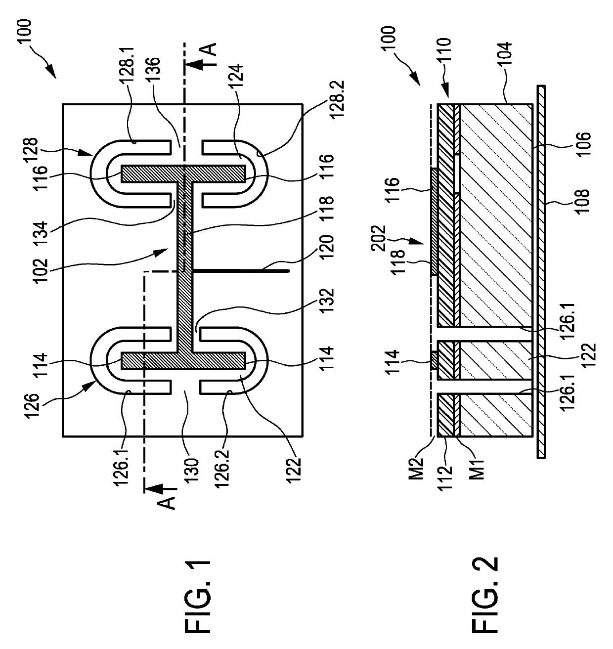
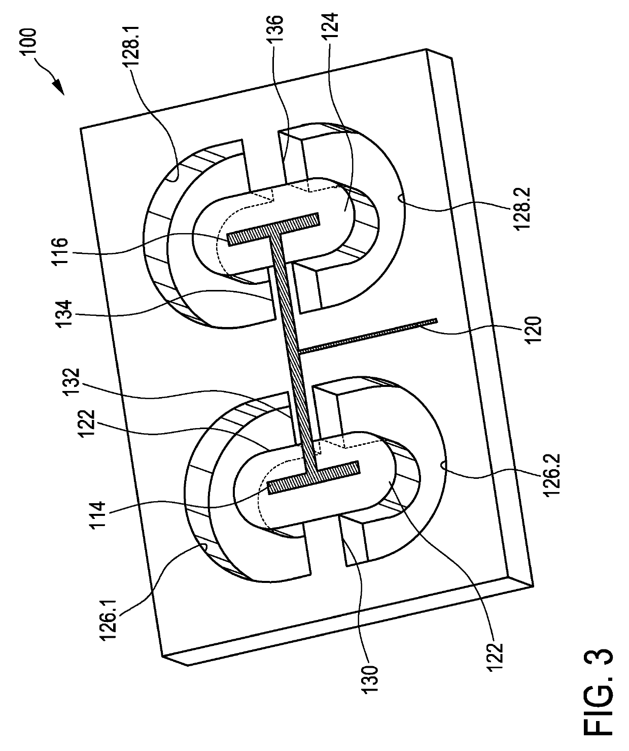
[0047]A first embodiment of a chip antenna 102 according to the present invention, integrated in an electronic component in the form of a chip 100, shall now be described with parallel reference to FIGS. 1 to 3. The views shown in FIGS. 1 to 3 are merely schematic. Each Figure shows only a lateral section of chip 100 containing chip antenna 102. Other lateral sections of chip 100, containing monolithically integrated electronic circuits, for example, are not shown in graphical form here for the sake of simplicity. In FIG. 3, some of the details drawn into the two views in FIGS. 1 and 2 have been left out. This is done solely for the purpose of clearer presentation.

[0048]Chip antenna 102 is formed on a semiconductor substrate, which is a silicon wafer 104 here. Silicon wafer 104 is a standard semiconductor substrate use in CMOS or BiCMOS processes.

[0049]Silicon wafer 104 is connected here by its underside 106 to a metallic reflector 108. The reflector can be a grounding surface of a ...


PUM


Abstract

A chip antenna comprising at least one emitter which extends parallel to a main surface of a semiconductor substrate supporting the chip antenna, wherein the emitter is arranged on an island-like support zone of the semiconductor substrate, the support zone being surrounded by at least one trench which is completely filled with a gas, the trench passing through the entire depth of the semiconductor substrate and being bridged by at least one retaining web which forms a supporting connection between the support zone and the rest of the semiconductor substrate.

Description

CROSS REFERENCE TO RELATED APPLICATIONS[0001]This application is the U.S. National Stage of International Application Number PCT / EP2013 / 077951 filed on Dec. 23, 2013, which application claims priority under 35 USC § 119 to German Patent Application No. 10 2012 224 458.1 filed on Dec. 27, 2012 and German Patent Application No. 10 2013 207829.3 filed on Apr. 29, 2013, which applications are hereby incorporated by reference in their entirety.TECHNICAL FIELD[0002]The invention relates to a chip antenna, an electronic component having a chip antenna, and a method for producing such a chip antenna.BACKGROUND OF THE INVENTION[0003]Such chip antennas are also referred to as on-chip antennas. They are used, in particular, in wireless transmission systems that operate with millimeter waves up to the a terahertz range. An increasing number of applications can be found in the fields of radar, fast data transfer, imaging systems and sensors.[0004]At the extremely high frequencies referred to abo...

Claims


Application Information

Patent Timeline
Patent Type & Authority Patents(United States)
IPC IPC(8): H01Q1/38H01Q21/00H01Q1/42H01L23/522H01Q21/06H01Q1/22H01L23/66H01Q19/10
CPCH01Q1/42H01Q21/0093H01L23/5227H01L23/66H01Q21/062H01Q1/38H01Q1/2283H01Q19/10H01L2924/0002H01L2924/00H01L2223/6677
Inventor WANG, RUOYUSUN, YAOMINGSCHEYTT, JOHANN CHRISTOPHKAYNAK, MEHMET
Owner IHP GMBH INNOVATIONS FOR HIGH PERFORMANCE MICROELECTRONICS LEIBNIZ INST FUR INNOVATIVE
Why Eureka
Try Eureka