Semiconductor device

a technology of semiconductor devices and semiconductors, applied in semiconductor devices, semiconductor/solid-state device details, electrical devices, etc., can solve the problems of difficult resin injection between wires and die pads, liable to occur peeling between mold resin and the back of chip mounting surfaces of die pads, etc., to achieve easy resin injection and easy chip alignment.

Active Publication Date: 2011-03-29
RENESAS ELECTRONICS CORP
View PDF5 Cites 1 Cited by
  • Summary
  • Abstract
  • Description
  • Claims
  • Application Information

AI Technical Summary

Benefits of technology

[0008]The present invention has been implemented to solve the above described problems and it is an object of the present invention to provide a semiconductor device in which two chips are mounted side by side and the two chips are directly interconnected using a wire, capable of preventing resin sealing leakage.
[0009]It is another object of the present invention to provide a semiconductor device that makes it easier, when two chips are mounted side by side on a die pad, to align the chips.
[0011]The semiconductor device according to this embodiment provides the mark in the bar provided between the first and second chips, and the plurality of inner leads, and thereby makes it easier to align the chips when mounting the two chips side by side on the die pad.
[0012]Furthermore, in the semiconductor device according to the other embodiment, since the width of the coupling part (third part) that couples the mounting parts (first and second parts) of the mounting member for mounting the two chips arranged apart from each other is made smaller than the widths of the mounting parts, it is easier to inject resin below the wire that connects the chips.

Problems solved by technology

Since the degree of adhesion between mold resin with which a semiconductor chip is sealed and a metallic die pad is generally not high, peeling is liable to occur between the mold resin and the back of the chip mounting surface of the die pad.
When resin sealing is applied, since this wire prevents a resin flow, it is difficult for resin to be injected between the wire and die pad.

Method used


Image

  • Semiconductor device
  • Semiconductor device
  • Semiconductor device

Examples


first embodiment

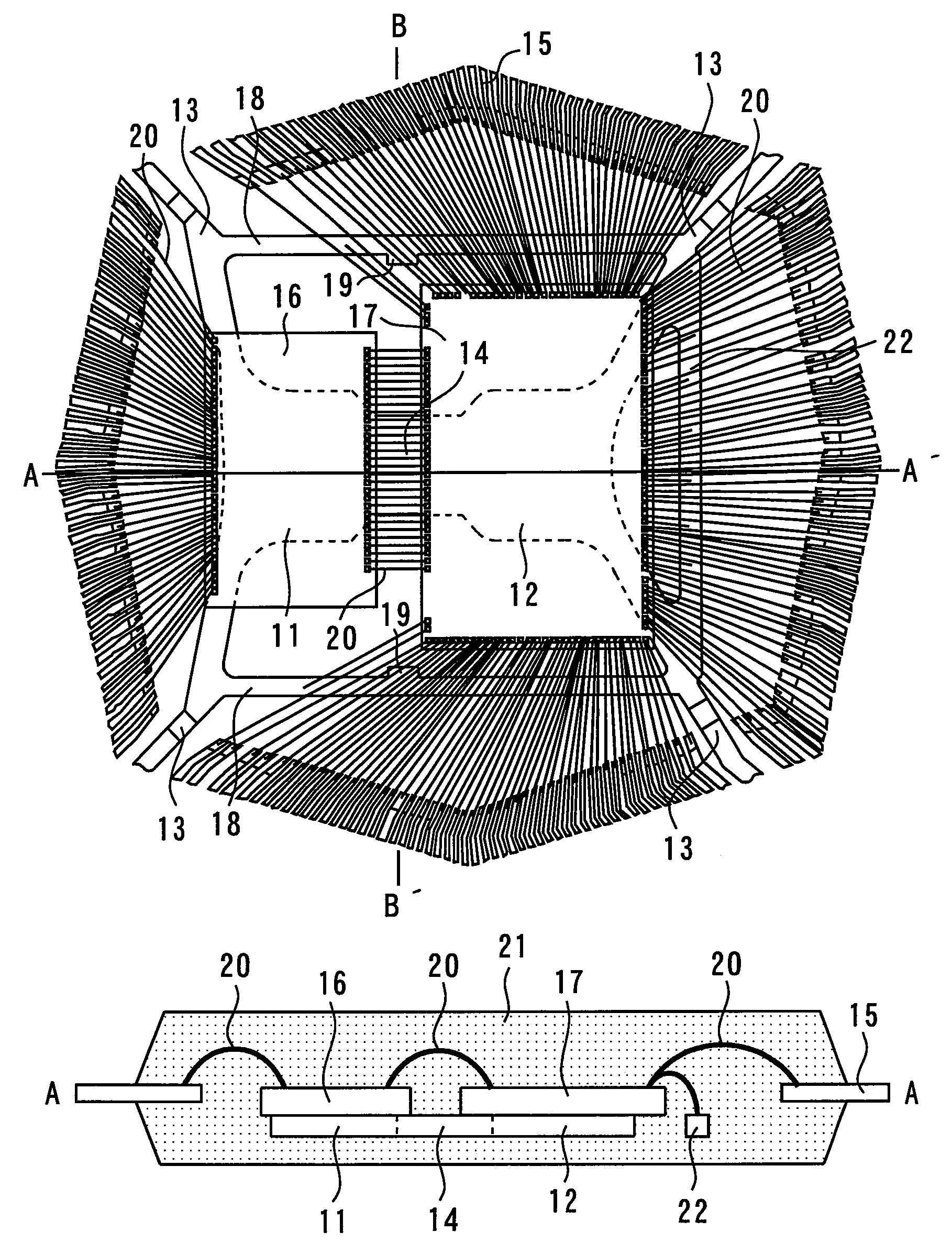
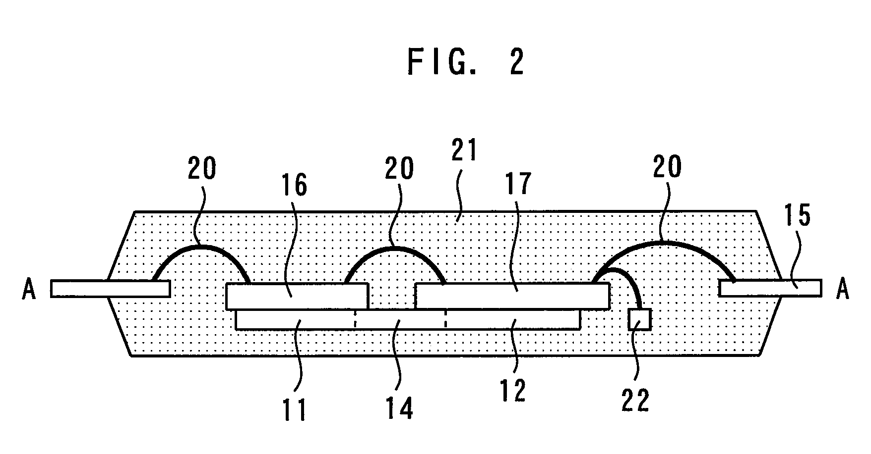
[0023]FIG. 1 is a plan view showing the interior of a semiconductor device according to an embodiment of the present invention, FIG. 2 is a cross-sectional view along A-A′ of FIG. 1. FIG. 10 is a cross-sectional view along B-B′ of FIG. 1. A first die pad 11 (first part) and a second die pad 12 (second part) are arranged side by side. The first and second die pads 11 and 12 are supported by hanger leads 13 and both pads are interconnected by a connection lead 14. The first and second die pads 11 and 12, connection lead 14 and hanger leads 13 constitute a metallic mounting member in which metal members are integrally molded. A plurality of inner leads 15 are arranged around the first and second die pads 11 and 12.

[0024]A first chip 16 is mounted with its principal plane superimposed on the first die pad 11 on the principal plane of the first die pad 11 by means of a paste (not shown). Furthermore, a second chip 17 is mounted with its principal plane superimposed on the principal plane...

second embodiment

[0047]In this second embodiment, as shown in FIG. 7, recessed parts 24 are provided in the connection lead 14 as marks instead of providing the marks in the bars 18 as in the case of the first embodiment. That is, the mounting member has the connection lead 14 (third part) located between the first and second chips 16 and 17 for coupling the first die pad 11 (first part) and the second die pad 12 (second part). The sides where the first die pad 11 is contiguous to the second die pad 12 via the connection lead 14 are provided with recessed parts 24 which are recessed in an inward direction of the sides. The bottom face of this recessed part 24 is located at least at the connection lead 14. As shown in FIG. 8, the first and second chips 16 and 17 are mounted on the die pads 11 and 12. The rest of the configuration is the same as that of the first embodiment. When the chips 16 and 17 are mounted on the die pads, the use of the recessed parts 24 as marks in this way makes it easier to a...


PUM


Abstract

A semiconductor device comprises: a first and second die pads arranged side by side; a plurality of inner leads arranged around the first and second die pads; first and second chips mounted on the first and second die pads; a bar provided between the first and second chips and the plurality of inner leads, extending in an array direction of the first chip and the second chip; a plurality of wires that connect the first and second chips and the plurality of inner leads and connect the first chip and the second chip; and resin that seals the first and second die pads, the plurality of inner leads, the first and second chips, the plurality of wires and the bar, wherein the bar comprises a mark provided at a position corresponding to an area between the first chip and the second chip in an array direction of the first chip and the second chip.

Description

BACKGROUND OF THE INVENTION[0001]1. Field of the Invention[0002]The present invention relates to a so-called SIP (System In Package) type semiconductor device in which two chips are mounted side by side on a die pad and sealed with resin.[0003]2. Background Art[0004]FIG. 9 is a plan view showing a conventional semiconductor device in which two chips are mounted side by side on a large die pad. Two chips 16 and 17 are mounted on a die pad 31. Here, the die pad 31 is larger than the chips 16 and 17. The chips 16 and 17 and a plurality of inner leads 15 are connected using a plurality of wires 20 and the chips 16 and 17 are interconnected. Slits 32 are formed in the die pad 31 between the chips 16 and 17. In the manufacturing process of this semiconductor device, when mounting the chips 16 and 17 on the die pad 31, the chips are aligned using the edge of the die pad 31 and the slits 32 as marks. Japanese Patent Laid-Open No. 2007-35853 describes a semiconductor device in which one chip...

Claims


Application Information

Patent Timeline
Patent Type & Authority Patents(United States)
IPC IPC(8): H01L23/495H01L21/50
CPCH01L23/49503H01L23/49575H01L24/49H01L2224/48091H01L2224/48137H01L2224/48247H01L2224/49171H01L2224/49175H01L2924/01005H01L2924/01057H01L2924/01082H01L2924/00014H01L24/48H01L2924/01006H01L2924/01033H01L2924/00H01L2924/181H01L2224/45099H01L2924/00012
Inventor MISUMI, KAZUYUKIHATAUCHI, KAZUSHI
Owner RENESAS ELECTRONICS CORP
Why Eureka
Try Eureka