RFID tag and method for manufacturing the same

a technology of radio frequency identification and rfid tag, which is applied in the direction of burglar alarm mechanical actuation, burglar alarm by hand-portable object removal, instruments, etc., can solve the problems of circuit chip detachment or disconnection, and counteract the demand for a thinner rfid tag

Inactive Publication Date: 2011-03-29
FUJITSU LTD
View PDF9 Cites 0 Cited by
  • Summary
  • Abstract
  • Description
  • Claims
  • Application Information

AI Technical Summary

Benefits of technology

[0018]The present invention has been made in view of the above circumstances and provides a thin RFID tag capable of sufficiently protecting its circuit chip against deformation, and a method of manufacturing the RFID tag.
[0025]In the RFID tag according to the present invention, the circuit chip included in the strap section is connected to the antenna of the antenna section through the second conductive pattern of the protection section larger in rigidity than the base of the antenna. Accordingly, even though the first base is made of a material that may be easily deformed, such deformation of the first base hardly affect the strap section because of relatively high rigidity of the protection section, thus preventing detachment of the circuit chip or disconnection of the circuit chip from the first conductive pattern. In the RFID tag according to the present invention, a stress caused by deformation of the first base is liable to concentrate on a connection part between the second conductive pattern of the protection section and the loop antenna of the antenna section. However, unlike a case in which the circuit chip is electrically connected to an external device through the tiny bump, and thus the contact area is limited, contact between the second conductive pattern and the antenna according to the present embodiment may be made at any contact area. By having the second conductive pattern electrically connected to the antenna in a contact area broader than the contact area between the circuit chip and the first conductive pattern as in the exemplary embodiment of the present invention, it is possible to make the connection part between the second conductive pattern of the protection section and the loop antenna of the antenna section have a sufficient resistance against concentrating stress caused by deformation of the first base. The protection section, serving to protect the circuit chip against deformation as described above, may be easily made thin, which in turn allows the overall RFID tag to be made thin, by forming the protection body with resin, for example, as in the exemplary embodiment of the present invention. Accordingly, a thin RFID tag may be obtained where the circuit chip may be sufficiently protected against deformation according to the present invention.
[0032]In the method of manufacturing the RFID tag according to the present invention, the connection between the second conductive pattern and the antenna may be made at any contact area, and therefore, the positioning of the protection section may be less precisely and easily performed in the mounting step, which is advantageous at the time of manufacturing. That is, the present invention enables a method of manufacturing a thin RFID tag where the circuit chip may be sufficiently protected against deformation according to the present invention.

Problems solved by technology

In this case, there could occur a problem as described below, such as detachment of the circuit chip or disconnection between the antenna and the circuit chip.
However, such a thickness of the resin layer counteracts the demand for a thinner RFID tag.

Method used


Image

  • RFID tag and method for manufacturing the same
  • RFID tag and method for manufacturing the same
  • RFID tag and method for manufacturing the same

Examples


Embodiment Construction

[0046]Hereinafter, embodiments of the present invention will be described in more detail with reference to accompanying drawings.

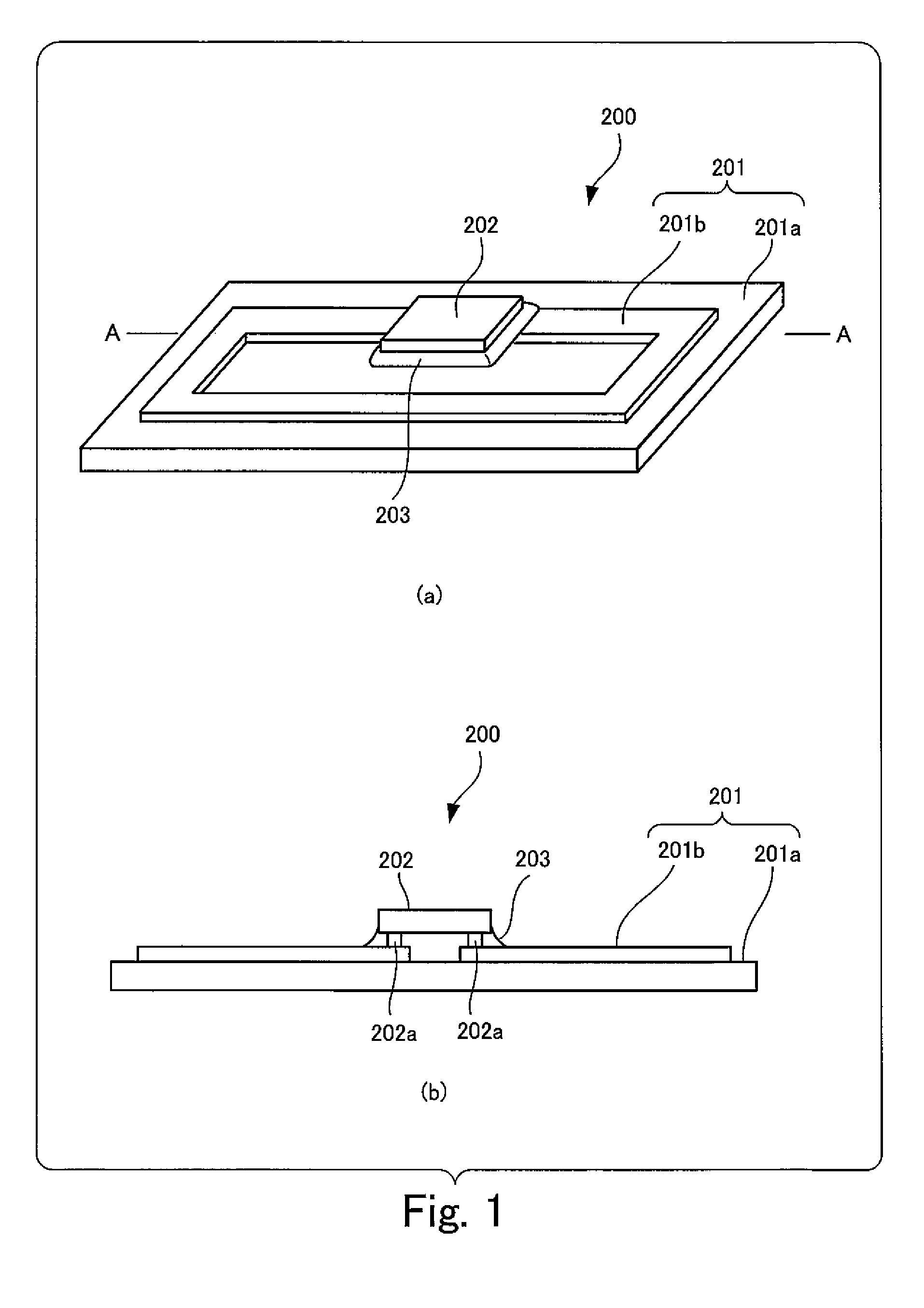
[0047]FIG. 5 is a view illustrating an RFID tag according to an embodiment of the present invention.

[0048]Part (a) of FIG. 5 depicts a perspective view of an exemplary RFID tag 100 according to an embodiment of the RFID tag of the present invention, and part (b) of FIG. 5 depicts a cross sectional view of the RFID tag 100 taken along the line B-B of Part (a) of FIG. 5.

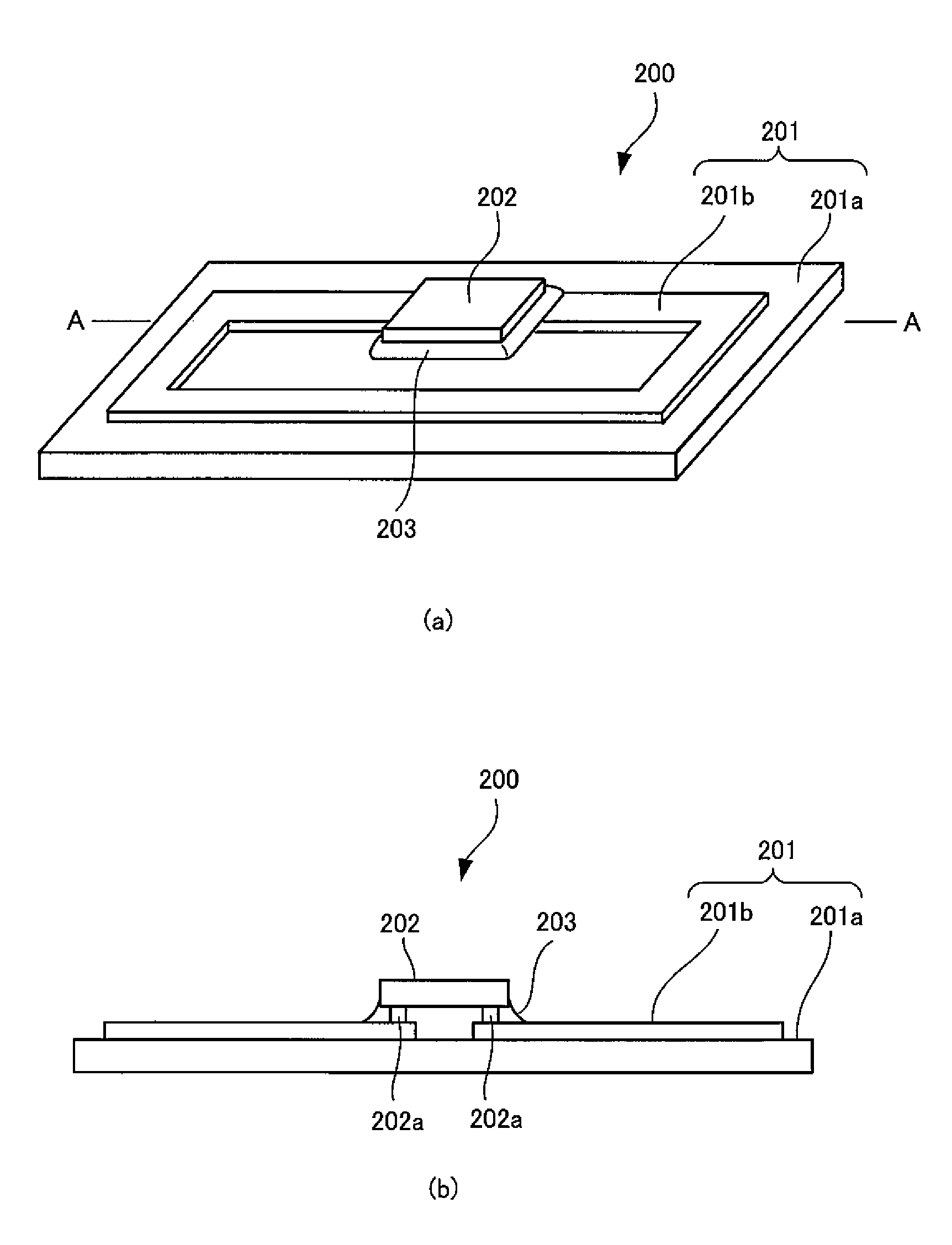
[0049]Referring to FIG. 5, the RFID tag 100 includes an antenna section 101, a strap section 102, and a protection section 103 as described in detail below. The antenna section 101, the strap section 102, and the protection section 103 correspond to an example of the antenna section, an example of the strap section, and an example of the protection section, respectively, of the present invention.

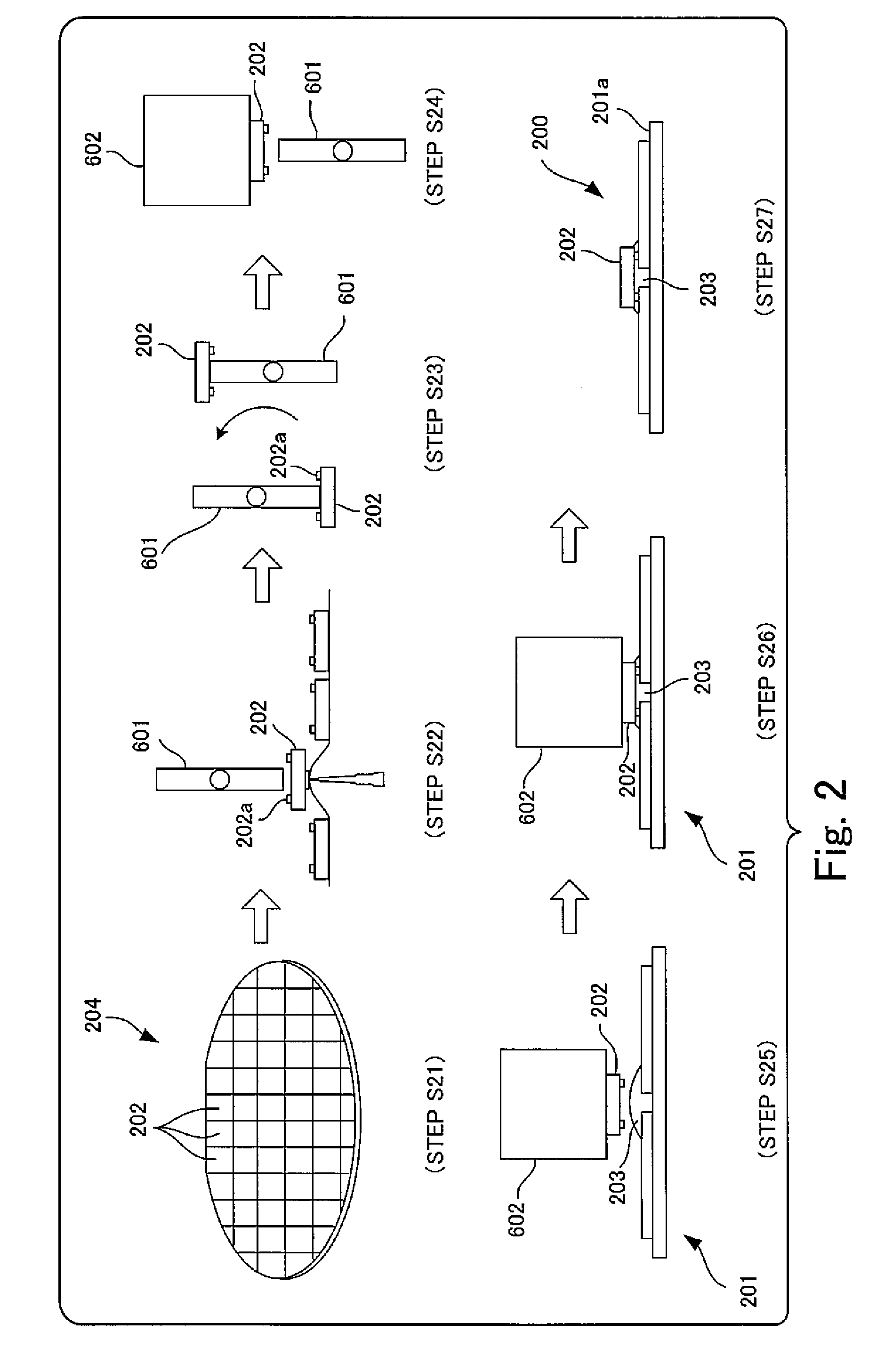
[0050]FIG. 6 is an exploded view of the RFID tag 100 shown in FIG. 5, wherein the RFID tag 100 is ...


PUM

PropertyMeasurementUnit
thicknessaaaaaaaaaa
thicknessaaaaaaaaaa
widthaaaaaaaaaa

Abstract

A RFID tag includes: an antenna section having a first base and a loop antenna; a strap section having a second base and a first conductive pattern to which a circuit chip is electrically connected; and a protection section having a protection body having relatively high rigidity and a second conductive pattern in which the protection body has a groove formed therein large enough to house the circuit chip, and the second conductive pattern electrically connects the first conductive pattern to the loop antenna.

Description

BACKGROUND OF THE INVENTION[0001]1. Field of the Invention[0002]The present invention relates to an RFID (Radio Frequency Identification) tag that contactlessly exchanges information with an external device and a method of manufacturing the RFID tag. As used herein, the term “RFID tag” may be also referred to as the term “wireless IC tag” by those skilled in the art.[0003]2. Description of Related Art[0004]A RFID tag is known, including a base made of plastic or paper and an antenna section arranged on the base and having an antenna for wireless communication, wherein a circuit chip is mounted on the antenna section, as a conventional RFID tag, which contactlessly exchanges information with an external device represented by a Reader / Writer.[0005]FIG. 1 is a view illustrating an exemplary RFID tag.[0006]Part (a) of FIG. 1 depicts a perspective view of an RFID tag 200, and Part (b) of FIG. 1 depicts a cross section of the RFID tag 200 taken along with line A-A of Part (a) of FIG. 1.[0...

Claims


Application Information

Patent Timeline
Patent Type & Authority Patents(United States)
IPC IPC(8): G08B13/00
CPCG06K19/07728G06K19/07749Y10T29/49016
Inventor ISHIKAWA, NAOKIKOBAYASHI, HIROSHI
Owner FUJITSU LTD
Why Eureka
Try Eureka