Memory device employing NVRAM and flash memory cells

a memory device and flash memory technology, applied in the field of memory devices, can solve the problems that the nand flash memory device b>100/b> may consume a relatively large amount of time performing a random access reading operation

Inactive Publication Date: 2011-03-29
SAMSUNG ELECTRONICS CO LTD
View PDF7 Cites 225 Cited by
  • Summary
  • Abstract
  • Description
  • Claims
  • Application Information

AI Technical Summary

Problems solved by technology

Accordingly, the NAND flash memory device 100 may consume a relatively large amount of time performing a random access reading operation.

Method used


Image

  • Memory device employing NVRAM and flash memory cells
  • Memory device employing NVRAM and flash memory cells
  • Memory device employing NVRAM and flash memory cells

Examples


Embodiment Construction

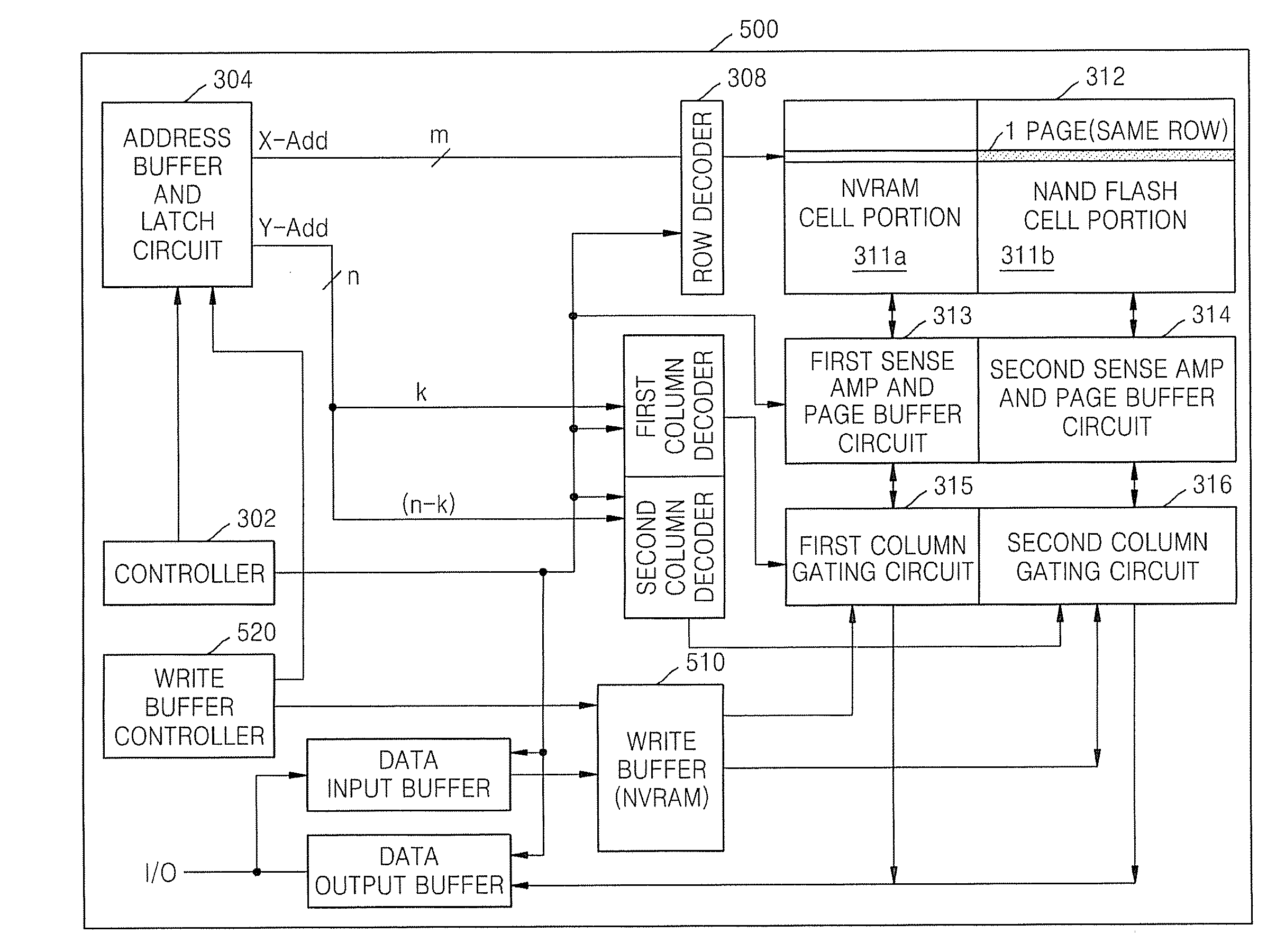
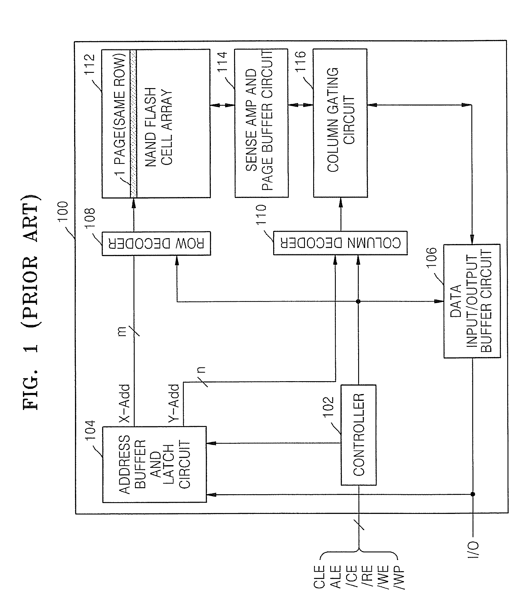
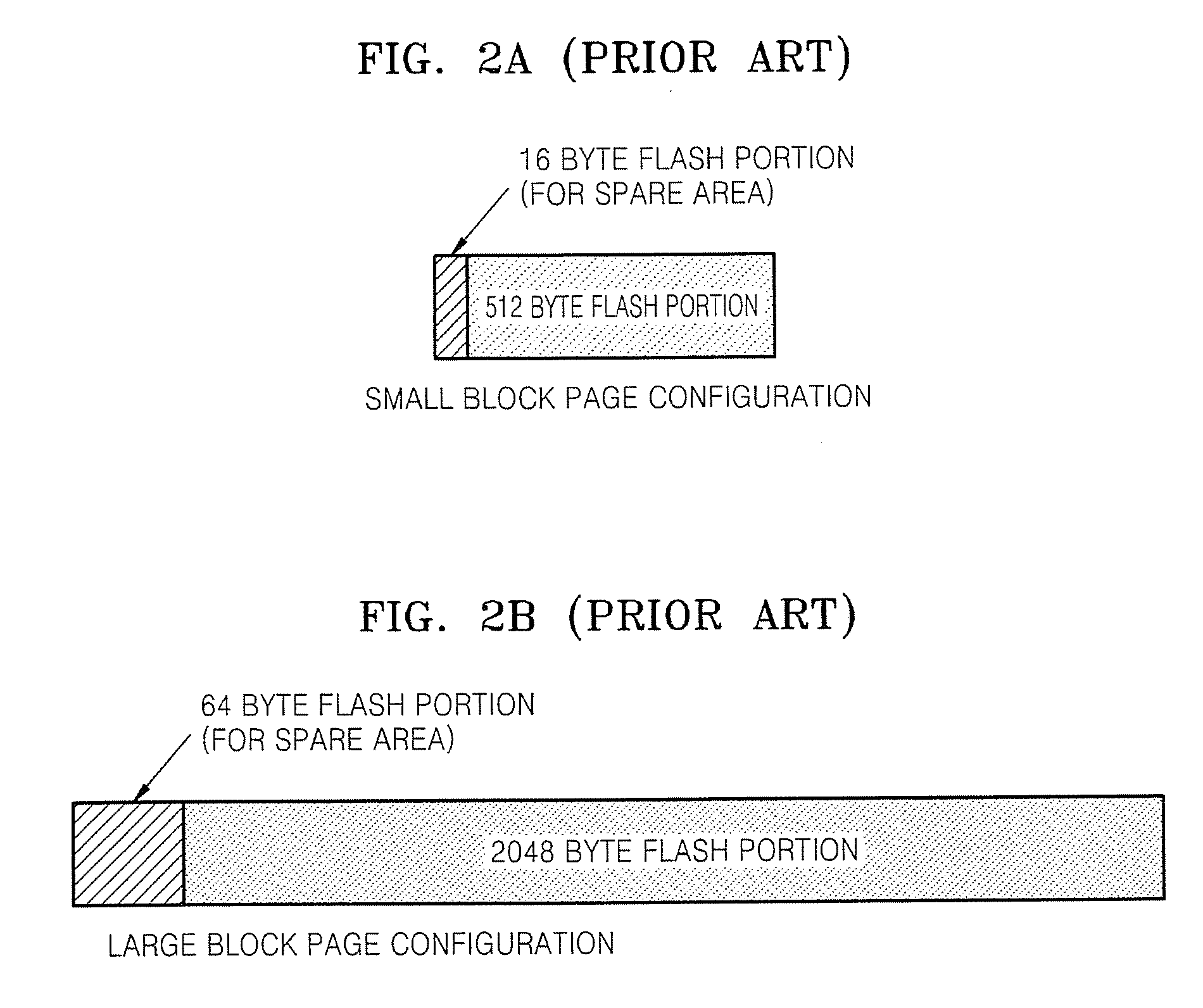
[0023]The present invention will now be described more fully hereinafter with reference to the accompanying drawings, in which exemplary embodiments of the invention are illustrated. The invention may, however, be embodied in different forms and should not be construed as limited to the embodiments set forth herein. Rather, these embodiments are provided so that this disclosure will be thorough and complete, and will fully convey the scope of the invention to those skilled in the art.

[0024]It will be understood that when an element is referred to as being on, connected to and / or coupled to another element, the element may be directly on, connected and / or coupled to the other element, or intervening elements may be present. In contrast, when an element is referred to as being directly on, directly connected to and / or directly coupled to another element, no intervening elements are present. As used herein, the term “and / or” includes any and all combinations of one or more of the assoc...


PUM


Abstract

A memory device includes a memory cell array including a NAND flash cell portion including a plurality of first columns of serially-connected flash memory cells and a non-volatile random access memory (NVRAM) cell portion including a plurality of second columns of NVRAM cells. The flash memory cells and the NVRAM cells are arranged such that respective word lines are connected to flash memory cells and NVRAM cells in each of respective rows, which may correspond to page units including flash memory cells and NVRAM cells.

Description

CROSS-REFERENCE TO RELATED PATENT APPLICATION[0001]This application claims the benefit of Korean Patent Application No. 10-2008-0008731, filed on Jan. 28, 2008, in the Korean Intellectual Property Office, the disclosure of which is incorporated herein in its entirety by reference.FIELD OF THE INVENTION[0002]The present invention relates to memory devices, and more particularly, to NAND flash memory devices.BACKGROUND OF THE INVENTION[0003]Flash memory devices typically program and erase data by using a tunneling phenomenon. Flash memory devices may be suitable for use as storage devices in portable media devices, because of their generally excellent data integrity, low power consumption, and strong durability from an external impact.[0004]NAND flash memory devices, in which memory cells are connected in series, may provide superior integration because the size of the memory cells may be kept relatively small as compared to NOR flash memory devices, in which memory cells are connecte...

Claims


Application Information

Patent Timeline
Patent Type & Authority Patents(United States)
IPC IPC(8): G11C16/04
CPCG11C11/005G11C16/0416G11C16/0483G11C16/02G11C16/06
Inventor JEON, BYUNG-GILMIN, BYUNG-JUNJEONG, HONG-SIK
Owner SAMSUNG ELECTRONICS CO LTD
Why Eureka
Try Eureka