Switching regulator configured to detect and shutdown reverse current
a switching regulator and reverse current technology, applied in the direction of electric variable regulation, process and machine control, instruments, etc., can solve the problems of reducing the the b>100/b> performance efficiency of the switching regulator
- Summary
- Abstract
- Description
- Claims
- Application Information
AI Technical Summary
Benefits of technology
Problems solved by technology
Method used
Image
Examples
first embodiment
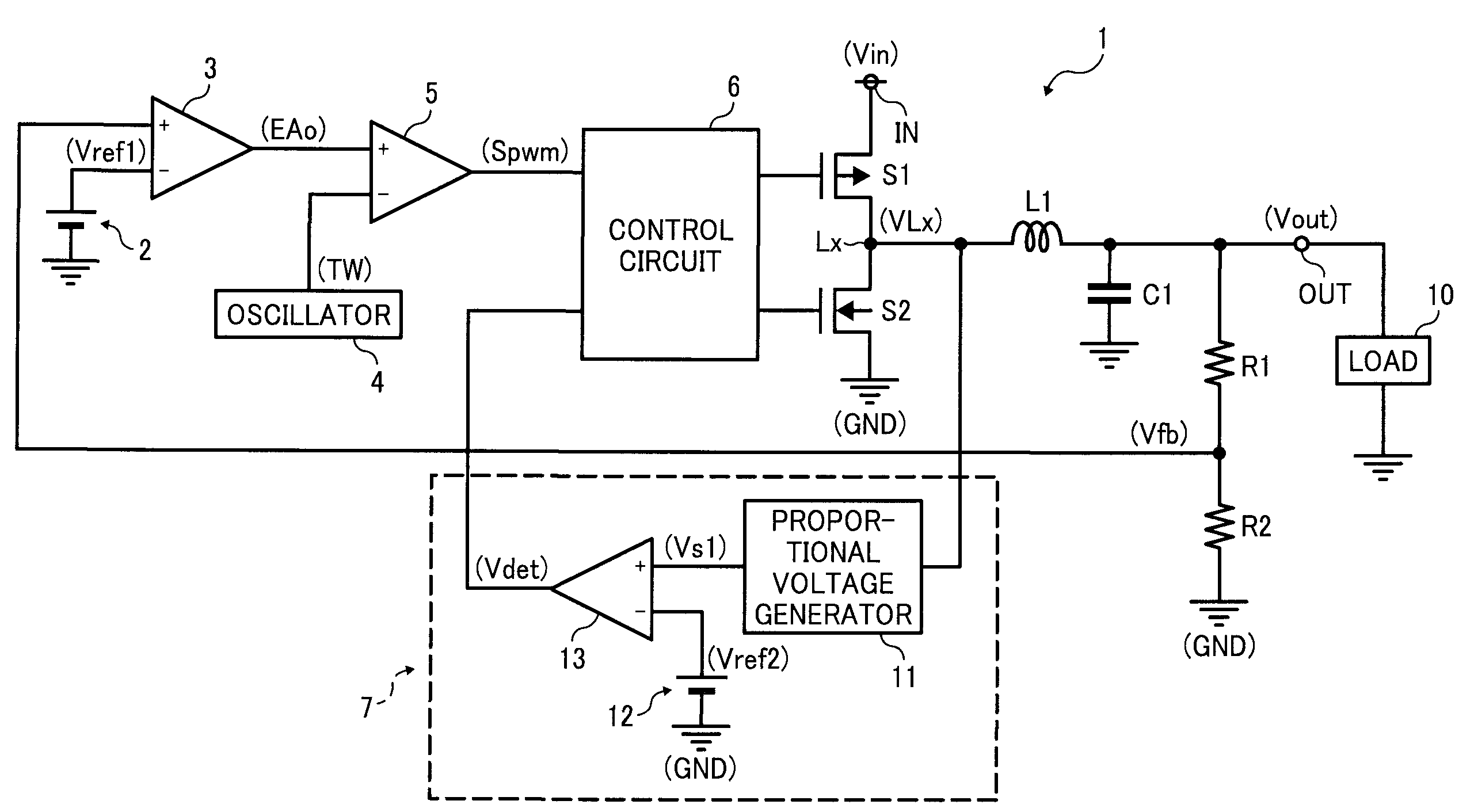
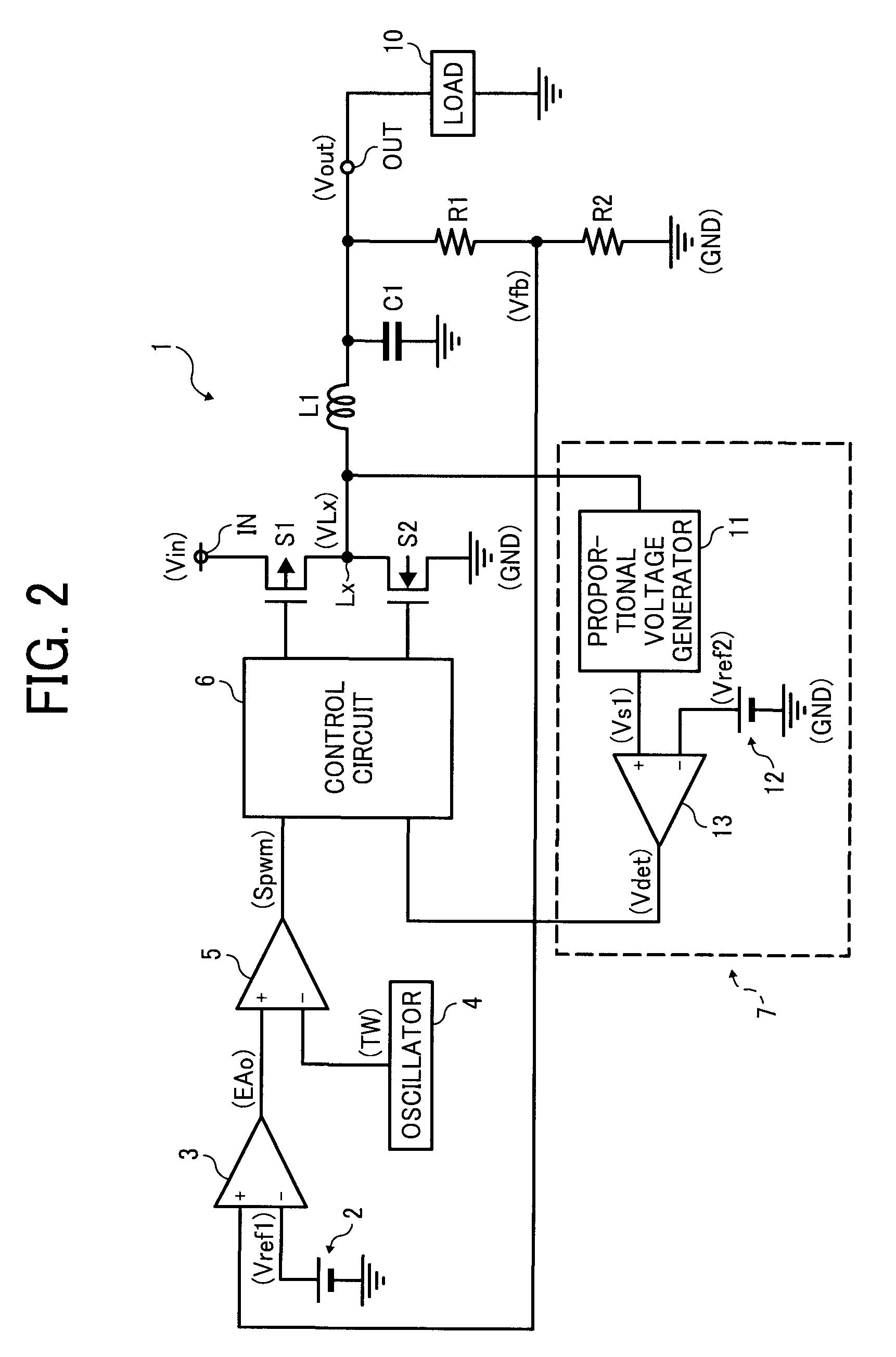
[0026]FIG. 2 is a circuit diagram of a switching regulator according to a first example embodiment. The switching regulator 1 is a step-down switching regulator that converts an input voltage Vin input at an input terminal IN to a predetermined voltage, and outputs the converted voltage as an output voltage Vout from an output terminal OUT to a load 10. The switching regulator 1 includes a switching transistor S1 and a synchronous rectification transistor S2. The switching transistor S1 is a PMOS transistor, and performs a switching operation to control output of the input voltage Vin. The synchronous rectification transistor S2 is an NMOS transistor.
[0027]Further, the switching regulator 1 includes a first reference voltage generator 2, resistors R1 and R2, an inductor L1, an error amplifier 3, an oscillator 4, a PWM comparator 5, a control circuit 6, and a reverse current detector 7. The resistors R1 and R2 detect the output voltage Vout, and the control circuit 6 controls the swi...
second embodiment
[0057]In the switching regulator according to the first example embodiment, the second reference voltage Vref2 is input to the inversion terminal of the comparator 13. However, in a switching regulator according to a second example embodiment, a reference voltage Vs2, which is obtained by adding a predetermined voltage V1 to the voltage VLx, is used for input to the inversion terminal of the comparator 13.
[0058]FIG. 6 is a circuit diagram of the switching regulator 1a according to the second example embodiment. In FIG. 6, identical reference characters are assigned to circuit members that are identical or similar to those shown in FIG. 2 and descriptions thereof are omitted.
[0059]The switching regulator 1a shown in FIG. 6 differs from the switching regulator 1 shown in FIG. 2 in that the second reference voltage generator 12 is removed and a reference voltage generator 21 is provided between the inversion terminal of the comparator 13 and the junction node Lx. Accordingly, the rever...
third embodiment
[0068]In the switching regulator according to the first example embodiment, the proportional voltage generator 11 generates and outputs a proportional voltage Vs1 proportional to the voltage VLx. In a switching regulator according to a third example embodiment, a proportional voltage Vs3 is created by multiplying the voltage VLx by a factor k, and a negative reference voltage −Vref3 is input to the inversion terminal of the comparator 13.
[0069]FIG. 9 is a circuit diagram of a switching regulator 1b according to the third example embodiment. In FIG. 9, identical reference characters are assigned to circuit members that are identical or similar to those shown in FIG. 2 and descriptions thereof are omitted.
[0070]The switching regulator 1b shown in FIG. 9 differs from the switching regulator 1 shown in FIG. 2 in that the proportional voltage generator 11 is replaced by a proportional voltage generator 31 which generates and outputs the proportional voltage Vs3 which is created by multip...
PUM
 Abstract
Description
Claims
Application Information


