Method for self-test and self-repair in a multi-chip package environment

a multi-chip package and environment technology, applied in the direction of electronic circuit testing, measurement devices, instruments, etc., can solve the problems of more difficult access to the integrated circuit within the multi-chip package than to the integrated circuit alone, and the testing of the integrated circuit within the multi-chip package may be more difficul

Inactive Publication Date: 2011-05-03
CHANGXIN MEMORY TECH INC
View PDF6 Cites 17 Cited by
  • Summary
  • Abstract
  • Description
  • Claims
  • Application Information

AI Technical Summary

Problems solved by technology

Where integrated circuits within an electronic device are placed within a multi-chip package, accessing the integrated circuits within the multi-chip packages may be more difficult than accessing the integrated circuits alone.
Because accessing the integrated circuits within the multi-chip package may be more difficult, testing of the integrated circuits within the multi-chip package may also be more difficult.

Method used


Image

  • Method for self-test and self-repair in a multi-chip package environment
  • Method for self-test and self-repair in a multi-chip package environment
  • Method for self-test and self-repair in a multi-chip package environment

Examples


Embodiment Construction

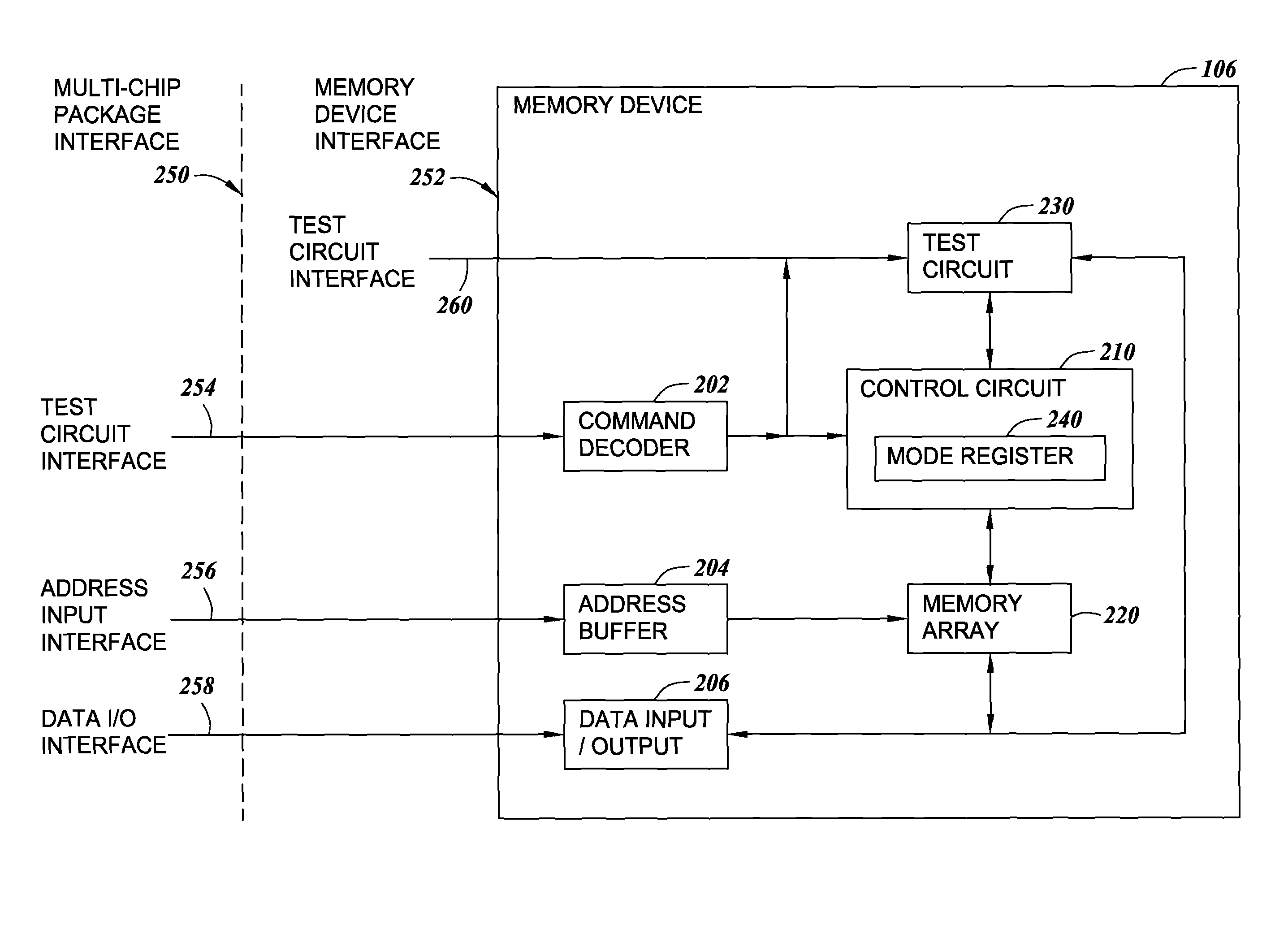
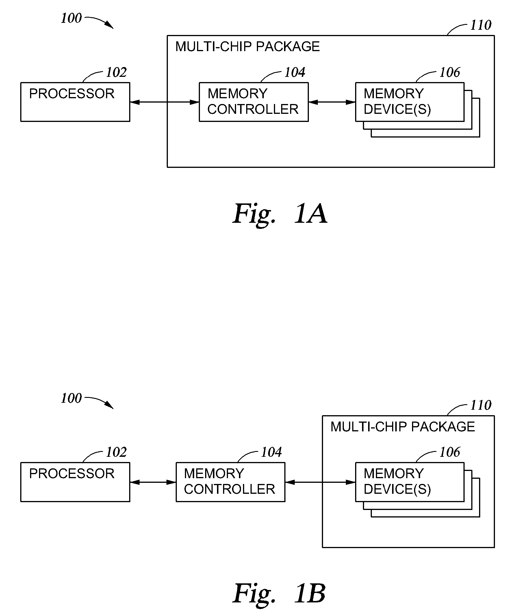
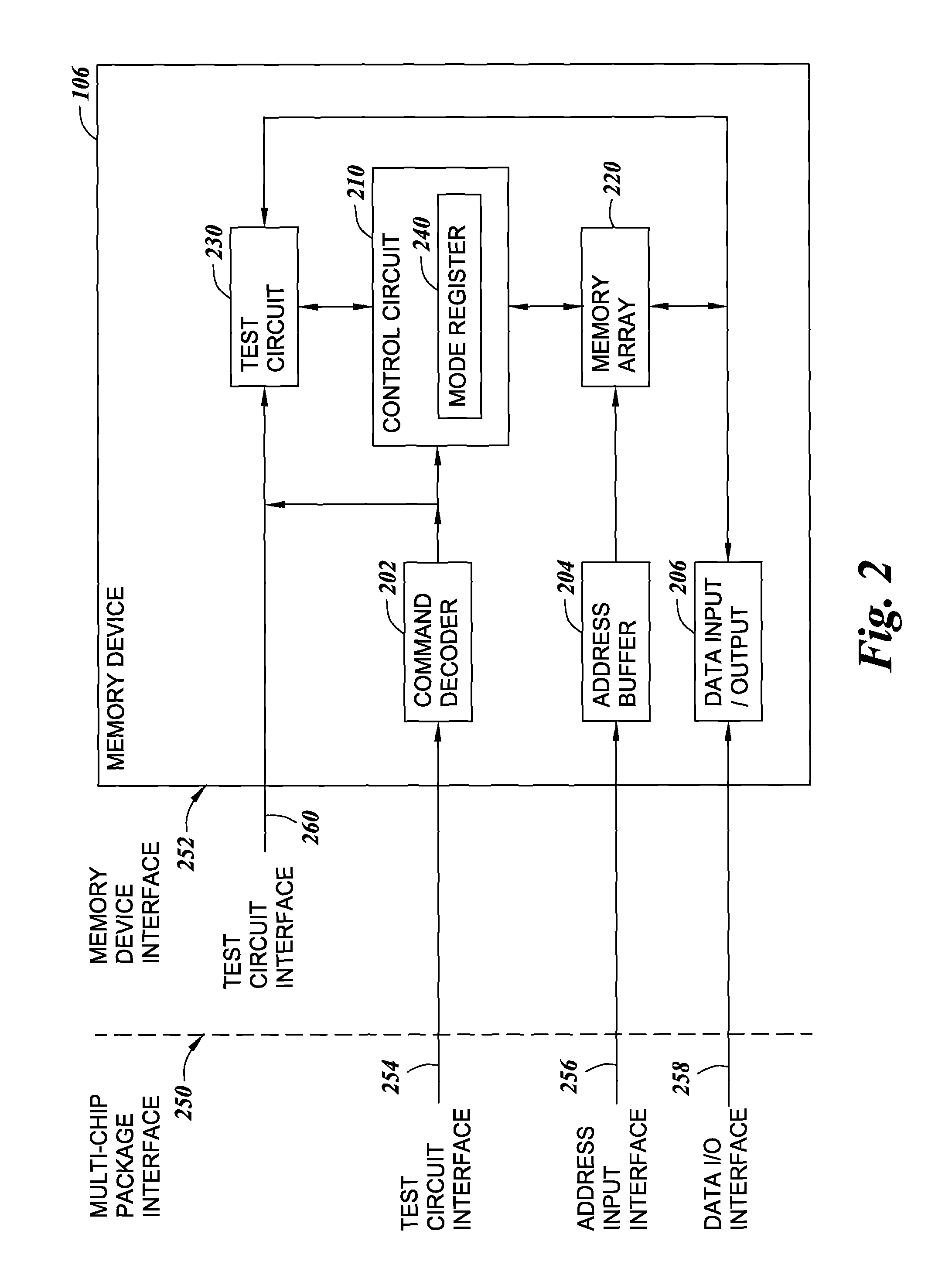
[0008]Embodiments of the invention generally provide a method and apparatus for operating a component including a memory device. The method includes receiving a plurality of commands and determining if a set of the plurality of commands matches a predefined pattern of commands configured to place the memory device into a test mode. Upon determining that the set of the plurality of commands matches the predefined plurality of commands, the memory device is placed in the test mode. In some cases, by using commands issued to the memory device to activate a test mode of the memory device, activation of the test mode may be achieved, even where access to a test interface of the memory device is restricted. Furthermore, in some cases, by using standard commands to activate the test mode of the memory device, systems including the memory device may be designed and tested without requiring extensive and / or expensive modifications of devices (e.g., memory controllers and / or processors) which...


PUM


Abstract

A method and apparatus for operating a component including a memory device. The method includes receiving a plurality of commands and determining if a set of the plurality of commands matches a predefined pattern of commands configured to place the memory device into a test mode. Upon determining that the set of the plurality of commands matches the predefined plurality of commands, the memory device is placed in the test mode.

Description

BACKGROUND OF THE INVENTION[0001]Modern electronic devices typically include several integrated circuits which perform functions for the electronic devices. The integrated circuits may include one or more processors, volatile memory devices, non-volatile memory devices, and / or memory controllers. In some cases, to reduce the cost of an electronic device and simplify development and manufacturing of the electronic device, one or more of the integrated circuits within the electronic device may be placed in a multi-chip package. For example, where a processor in an electronic device accesses one or more memory circuits using a memory controller, the one or more memory circuits and / or the memory controller may be placed in a multi-chip package (MCP).[0002]In order to ensure proper functioning of an electronic device, the integrated circuits within the electronic device may be subjected to one or more tests. Where integrated circuits within an electronic device are placed within a multi-...

Claims


Application Information

Patent Timeline
Patent Type & Authority Patents(United States)
IPC IPC(8): G11C29/00
CPCG11C29/4401G11C29/46G11C5/04G11C2029/0401G11C29/48
Inventor VOGELSANG, THOMAS
Owner CHANGXIN MEMORY TECH INC
Why Eureka
Try Eureka