Surface preparation for thin film growth by enhanced nucleation

a technology of enhanced nucleation and surface preparation, which is applied in the field of material deposition, can solve problems such as difficult nucleation, and achieve the effects of superior film growth, enhanced nucleation, and low energy

Active Publication Date: 2011-05-17
THE BOARD OF TRUSTEES OF THE UNIV OF ILLINOIS
View PDF50 Cites 30 Cited by
  • Summary
  • Abstract
  • Description
  • Claims
  • Application Information

AI Technical Summary

Benefits of technology

[0008]The processes provided herein yield superior film growth via enhanced nucleation and rely on the use of activated species of relatively low energy to achieve good nucleation without sputtering or otherwise damaging or degrading the surface. In this manner, uniform structures that are relatively thin can be reliably achieved, including thin films that are supported by an underlying receiving surface, without significantly impacting the surface as often occurs during conventional processing techniques including pretreatment processing. Substrate activation provided by the present methods provides for generation of uniform thin films, optionally conformal thin films, having low defect levels, and thin films having useful substrate-thin film interface properties.
[0009]The processes and systems described herein activate regions of the receiving surface of the substrate by activating the surface in a manner that avoids or at least substantially avoids etching or sputtering of the surface. Examples of species capable of such surface activation include output from a remote plasma of an inert gas such as, for example, a metastable species. To minimize unwanted interaction between the species, or an other material generated directly or indirectly from the species, the current at the receiving surface attributed to the introduced species can be monitored such that the current remains below a user-selected current density. Similarly, the energy of species provided for substrate activation by the remote plasma may be selected to remain below a user-selected energy level. As used herein, “activation” refers to surface treatment so as to enhance nucleation and growth of uniform films. The treatment may be a pretreatment where activation occurs prior to material deposition. The treatment may be a treatment that occurs during deposition. The treatment may comprise both a pretreatment and a treatment during deposition. Flux, duration of exposure, temperature are examples of other variables that may be optionally selected to further control process conditions to thereby influence final structure configuration and properties.
[0010]In general, various processes provided herein facilitate methods of surface activation by treatment without sputtering or other undesirable surface or substrate chemical interaction. The treatment affords a very high nucleation density and hence, fast coalescence during the film or structure deposition. By this treatment, in an aspect, a metal-based film on silicon is achieved that is fully coalesced of less than about 5 nm in thickness with a rms roughness less than about 1 nm. In an aspect, the treatment relates to exposing a surface to a metastable species, such as generated plasma of an inert or noble gas like argon, helium, neon, xenon and / or exposing a surface to high energy electromagnetic radiation such as photons sufficient to activate the surface, for example by photochemical and photothermal processes that remove H termination and generate dangling bonds. These species have sufficient energy to create nucleation sites on the substrate or otherwise enhance nucleation conditions but are of sufficiently low energy to not damage or remove surface atoms on the receiving surface.
[0011]Processes disclosed herein facilitate nucleation enhancement during thin film deposition following a surface treatment. The treatment involves exposure of the substrate to gaseous species (low energy ions, metastables, or electrons) and / or photons from a noble gas plasma generated outside the deposition chamber. Activation can be achieved via exposure of the surface to gaseous species (low energy ions, metastables, or electrons) and / or photons prior to thin film deposition or co-treatment via exposure of the surface to gaseous species (low energy ions, metastables, or electrons) and / or photons during thin film deposition. After or during the treatment, the substrate is exposed to the precursor molecule used in the CVD or ALD growth process. With the treatment of the substrate, the nucleation is very rapid, and fully coalesced films are achieved at a low film thickness. Without the treatment, nucleation is difficult and large islands form before coalescence is achieved. This is confirmed experimentally via atomic force microscopy (AFM) images of the film with and without treatment. With treatment, a typical roughness of a fully coalesced film has a root-mean-squared (rms) value of <7.5 Å, about three times less than for a film deposited without the treatment.
[0014]Any of the methods described herein can be further defined in terms of the energy of the remote plasma. In an embodiment, the remote plasma has an energy less than or equal to a user selected potential. Alternatively, the remote plasma has an energy selected over the range of 1 eV to 100 eV, or about 20 eV. In an embodiment, the remote plasma energy level is selected to achieve an electron energy level downstream such as in the deposition chamber of less than 1 eV, less than 0.5 eV, between 0.1 eV and 0.3 eV, or an energy level that avoids or minimizes unwanted surface substrate interactions.

Problems solved by technology

Without the treatment, nucleation is difficult and large islands form before coalescence is achieved.

Method used


Image

  • Surface preparation for thin film growth by enhanced nucleation
  • Surface preparation for thin film growth by enhanced nucleation
  • Surface preparation for thin film growth by enhanced nucleation

Examples


example 1

Schematic and Overview of Enhanced Nucleation

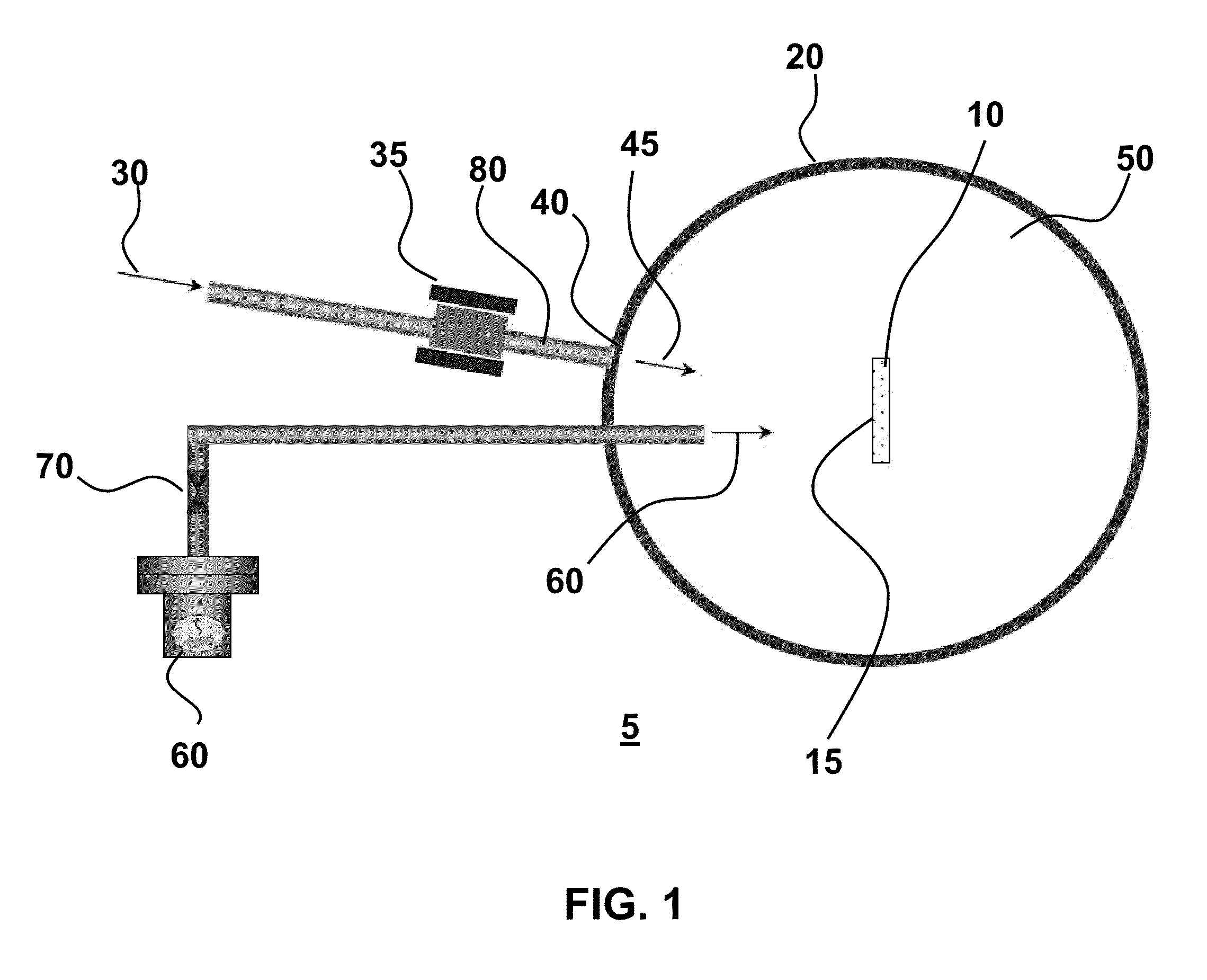
[0055]FIG. 1 is the schematic of a high vacuum reactor 5 used to generate high-quality thin films. The substrate 10 used in this example is silicon; prior to loading in chamber 20, it is dipped in dilute HF acid and rinsed with deionized water to passivate the surface by terminating the silicon bonds with hydrogen. This substrate 10 is then introduced via a load-lock into the reactor or chamber 20, which has been pumped to a base pressure of 10−8 Torr. The substrate is aligned with respect to a spectroscopic ellipsometer to observe changes in the optical properties of the film-on-substrate system during treatment and during film growth. The substrate is heated radiatively to 275° C. The ellipsometer data acquisition is turned on.

[0056]In a first set of experiments, Argon gas 30 flows into the chamber 20 through the remote plasma cavity orifice 40 downstream of the remote plasma generator 35. Conduit 80, such as a glass tube, conveys plasm...

example 2

Nucleation Enhancement During Thin Film Deposition

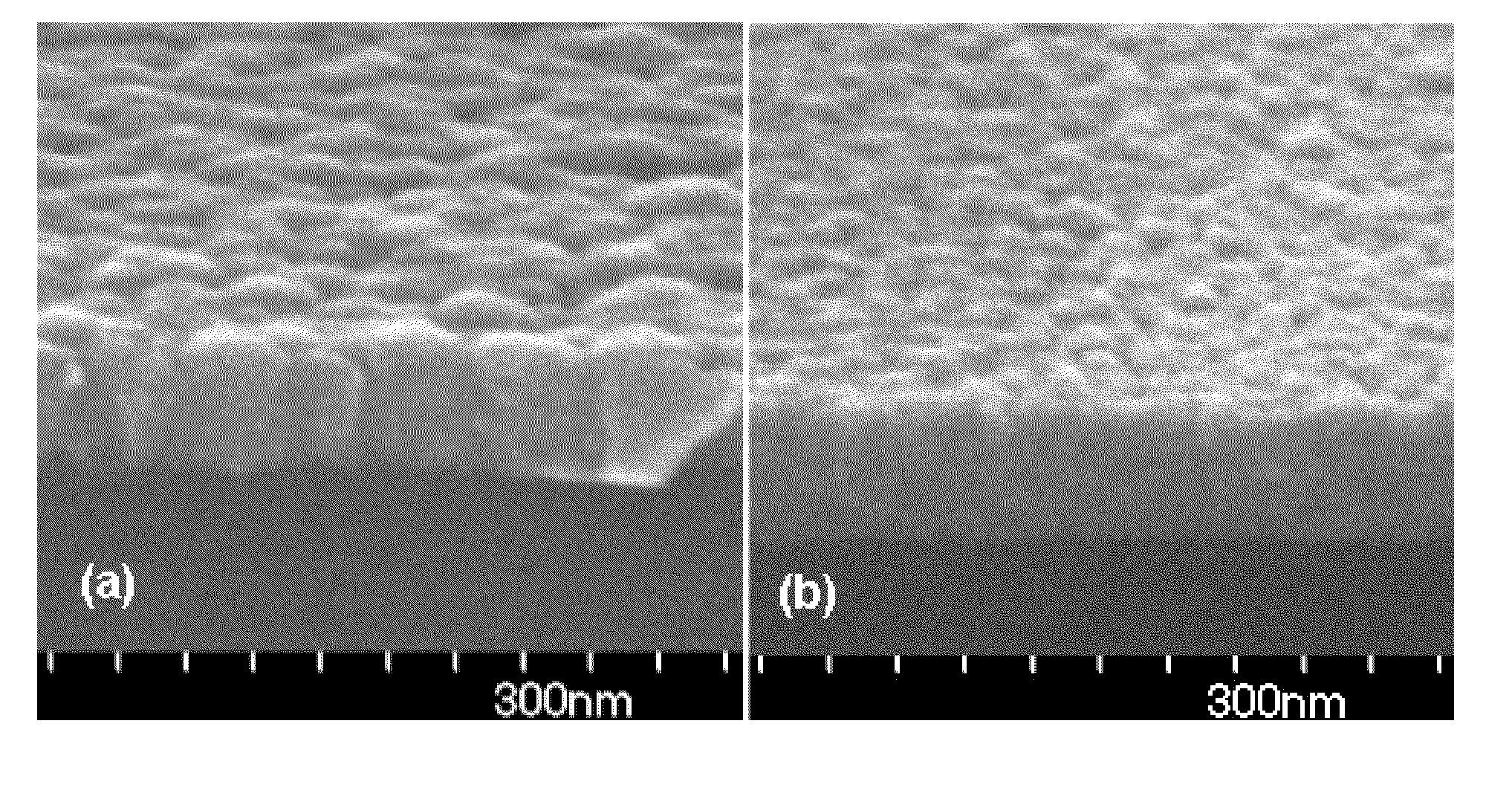
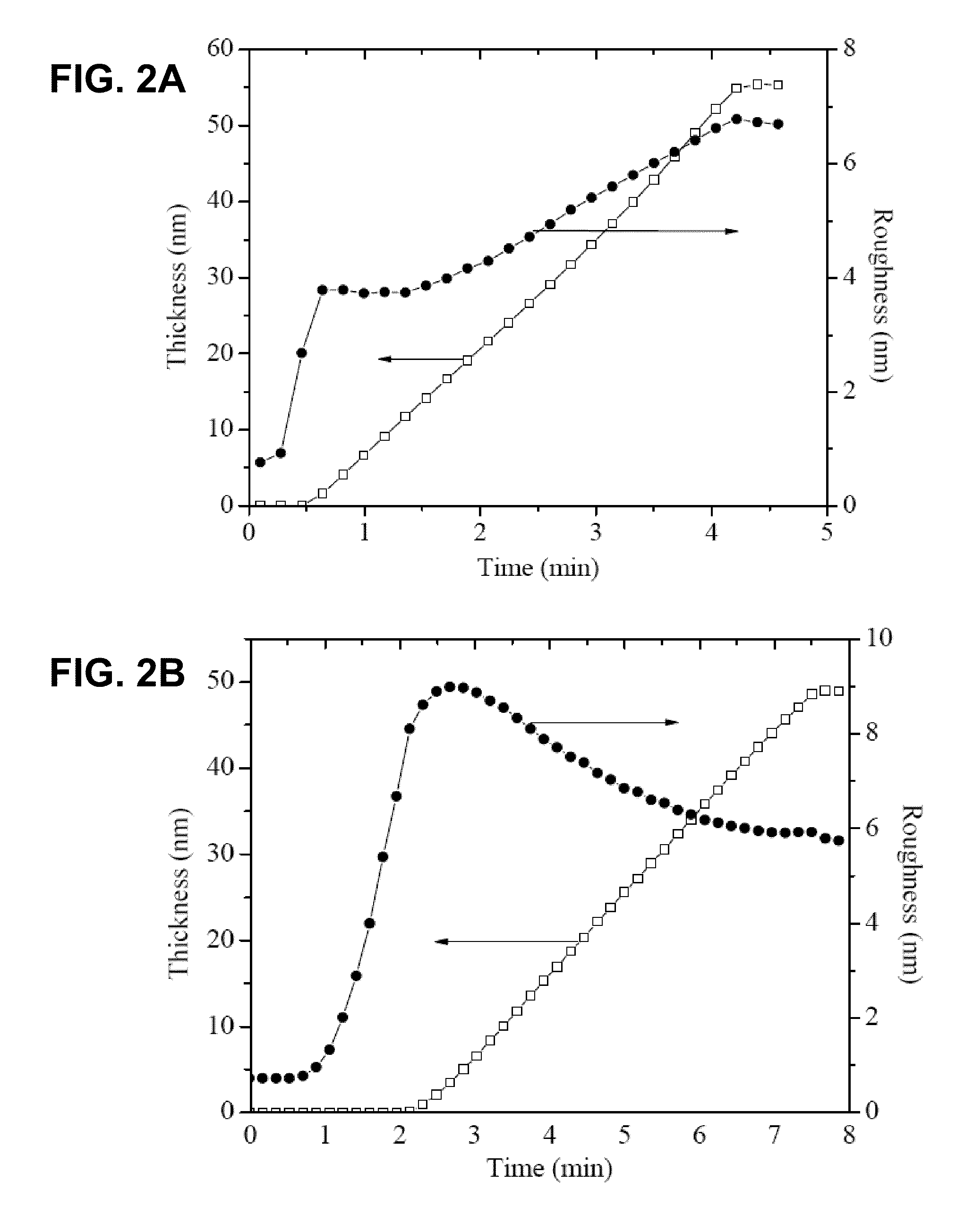
[0063]The requirement for ultra thin films in microelectronics and other applications in nanotechnology has made nucleation one of the primary focuses in thin film deposition.1 Dense nucleation and fast coalescence enables deposition of pinhole free ultra-thin smooth film. In CVD and ALD, two commonly used techniques for thin film deposition, nuclei are formed in selected sites on the substrate surface after which they grow and coalesce.2,3 With fewer of these nucleation sites, corresponding island sizes are larger and the time for fully-coalesced films increases. In such situations it is almost inevitable to get high roughness values with higher thicknesses before a fully coalesced film is formed. It is therefore imperative to have high nucleation density on the substrate surface, to grow fully coalesced ultra-thin films with low roughness values. Prior techniques of nucleation enhancement have been system (substrate, precursor) spe...


PUM

PropertyMeasurementUnit
energyaaaaaaaaaa
thicknessaaaaaaaaaa
root mean squared roughnessaaaaaaaaaa

Abstract

Various processes and related systems are provided for making structures on substrate surfaces. Disclosed are methods of making a structure supported by a substrate by providing a substrate having a receiving surface and exposing at least a portion of the receiving surface to output from a remote plasma of an inert gas. The remote plasma has an energy low enough to substantially avoid etching or sputtering of the receiving surface but sufficient to generate a treated receiving surface. The treated surface is contacted with a deposition gas, thereby making the structure supported by the substrate.

Description

CROSS-REFERENCE TO RELATED APPLICATIONS[0001]This application claims the benefit of U.S. provisional application 61 / 057,368 filed May 30, 2008, which is incorporated by reference in its entirety to the extent not inconsistent with the disclosure herein.BACKGROUND OF THE INVENTION[0002]Processes and systems provided herein generally relate to the field of material deposition. In particular, disclosed processes and systems provide for effective nucleation of thin films useful in various deposition techniques that grow material on a substrate to access formation of smooth and uniform thin films which may be used in microelectronics, MEMS, and other technologies.[0003]Chemical vapor deposition (CVD) is a common technique for depositing thin films for various applications including integrated circuits, MEMS, and hard coatings. Atomic layer deposition (ALD) is another such technique, which has the capability to deposit highly conformal and uniform coatings of controlled thickness. Both of...

Claims


Application Information

Patent Timeline
Patent Type & Authority Patents(United States)
IPC IPC(8): H01L21/31
CPCC23C16/0227H01L21/02315C23C16/50
Inventor KUMAR, NAVNEETYANGUAS-GIL, ANGELGIROLAMI, GREGORY S.ABELSON, JOHN R.
Owner THE BOARD OF TRUSTEES OF THE UNIV OF ILLINOIS
Why Eureka
Try Eureka