Semiconductor device having analog transistor with improved operating and flicker noise characteristics and method of making same

a technology of analog mos transistors and semiconductors, applied in the field of semiconductor devices, can solve the problems of ineffective methods to enhance the mobility of electrons and holes, inability to apply straining technology, and inability to improve the flicker noise characteristics of strained analog mos transistors

Active Publication Date: 2011-05-31
SAMSUNG ELECTRONICS CO LTD
View PDF15 Cites 121 Cited by
  • Summary
  • Abstract
  • Description
  • Claims
  • Application Information

AI Technical Summary

Problems solved by technology

However, strained analog MOS transistors tend to exhibit deteriorating flicker noise characteristics.
Even though straining technology may have the ability to enhance the mutual conductance and cut-off frequency characteristics of analog MOS transistors, it may not be the most effective method to enhance the mobility of electrons and holes.
In particular, in the case of large-scale integrated circuits (LSI) which comprise both digital and analog MOS transistors to provide completely integrated functions, it may be inappropriate to apply straining technology to both digital MOS transistors and analog MOS transistors at the same time.

Method used


Image

  • Semiconductor device having analog transistor with improved operating and flicker noise characteristics and method of making same
  • Semiconductor device having analog transistor with improved operating and flicker noise characteristics and method of making same
  • Semiconductor device having analog transistor with improved operating and flicker noise characteristics and method of making same

Examples


Embodiment Construction

[0015]The present invention will now be described more fully with reference to the accompanying drawings, in which preferred embodiments of the invention are shown. The invention may, however, be embodied in many different forms and should not be construed as being limited to the embodiments set forth herein. Rather, these embodiments are provided so that this disclosure will be thorough and complete, and will fully convey the scope of the invention to those skilled in the art. In the drawings, like numbers refer to like elements throughout.

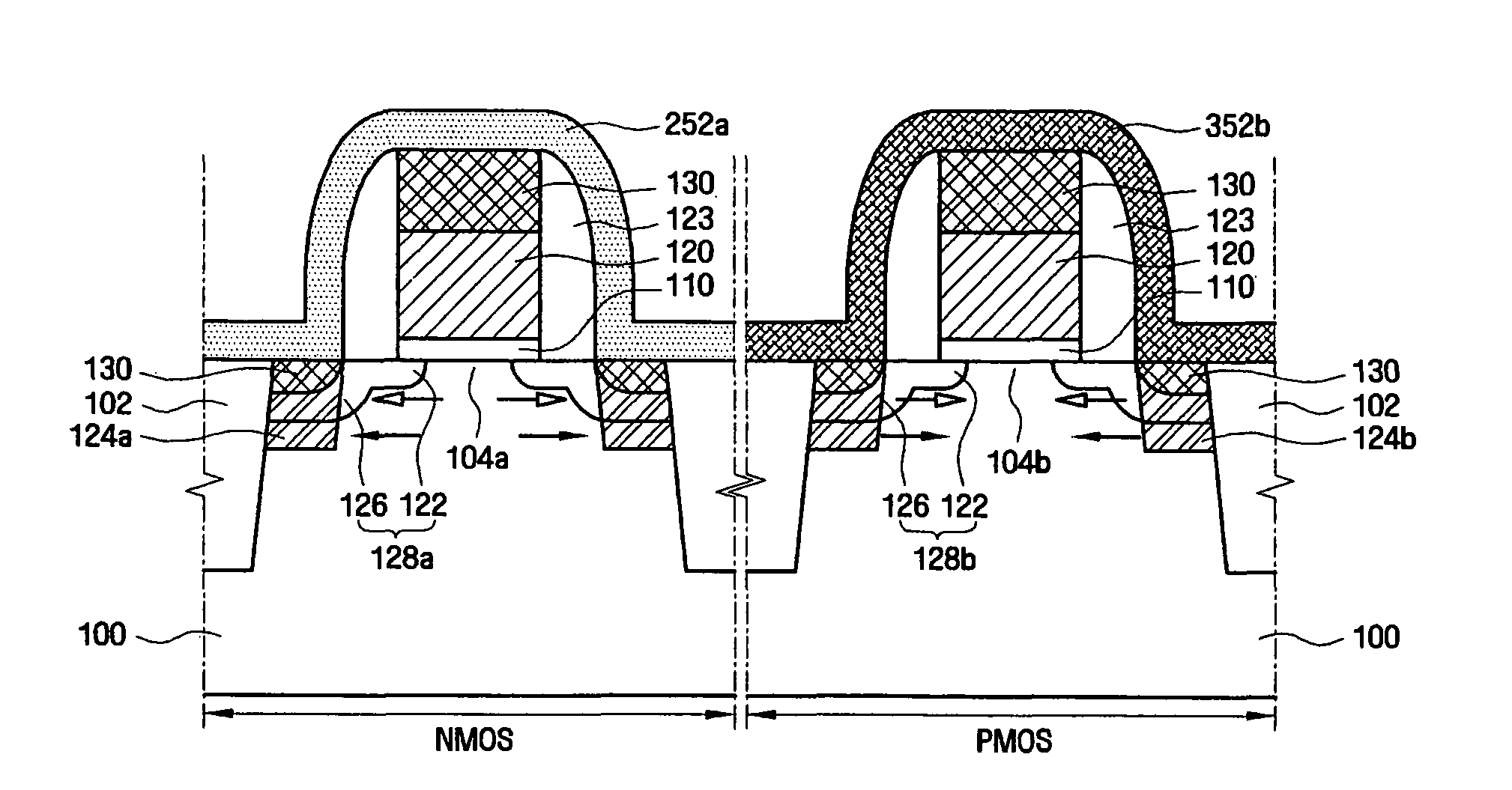
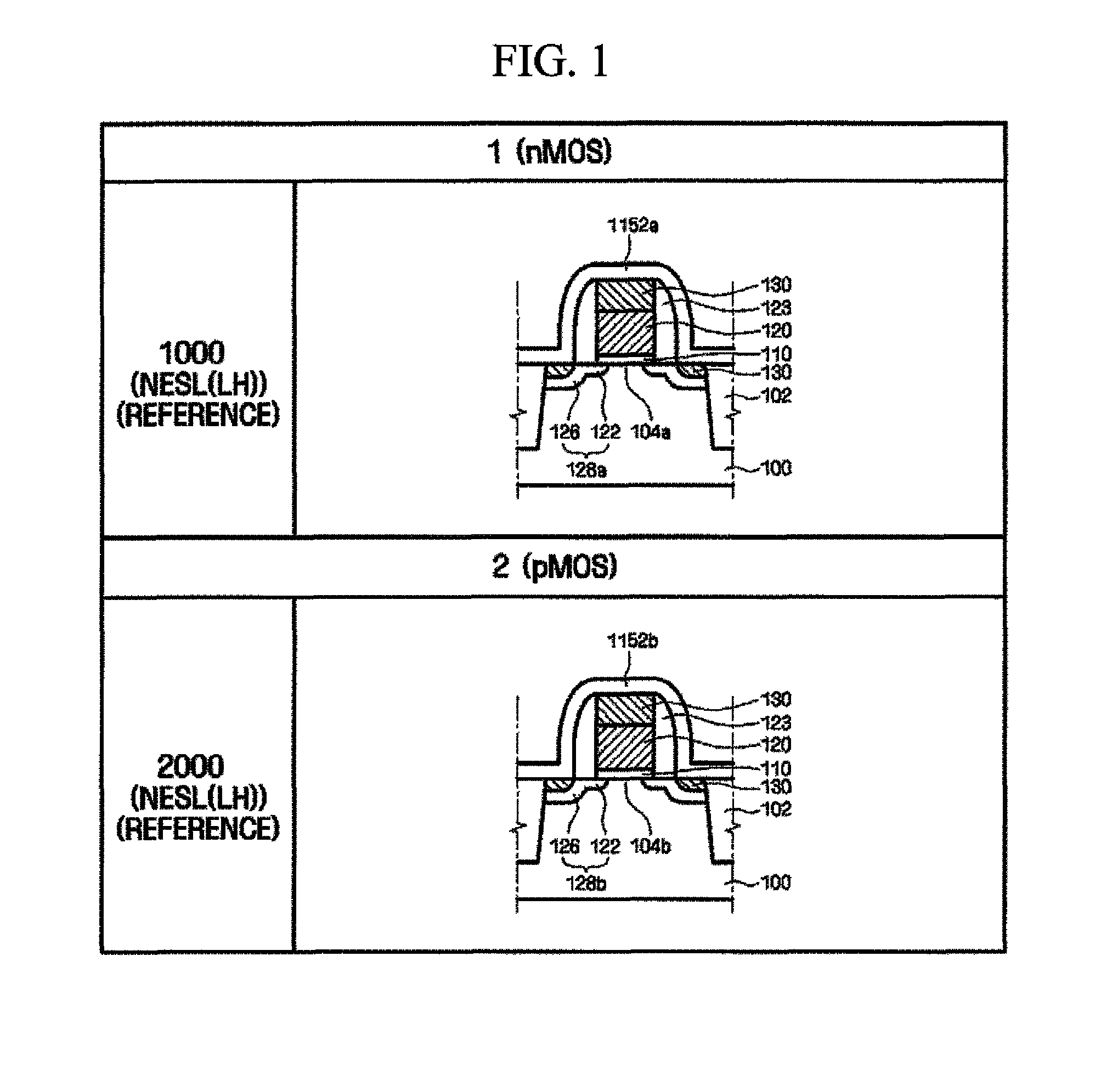
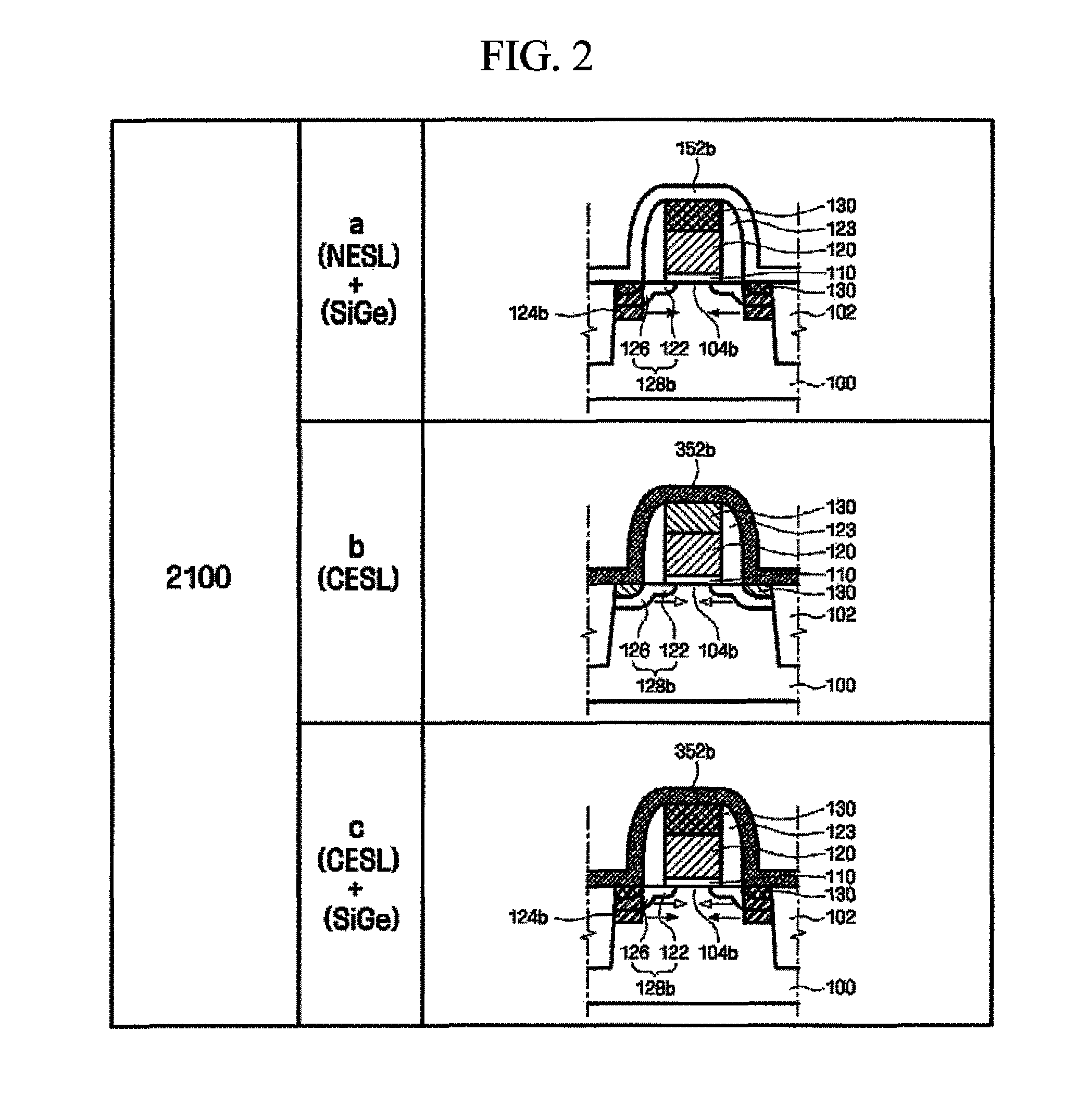
[0016]FIGS. 1-5 illustrate schematic views of semiconductor devices that include various combinations of strained-channel analog PMOS transistors 2100 of (FIG. 2) and strained or unstrained channel analog NMOS transistors 3100, 4100, and 5100 (FIGS. 3-5). Strained channels are obtained by applying compressive or tensile stress to typical channels so that the mobility μ of carriers (electrons or holes) can be changed. The relative measurement of t...


PUM


Abstract

A semiconductor device with improved transistor operating and flicker noise characteristics includes a substrate, an analog NMOS transistor and a compressively-strained-channel analog PMOS transistor disposed on the substrate. The device also includes a first etch stop liner (ESL) and a second ESL which respectively cover the NMOS transistor and the PMOS transistor. The relative measurement of flicker noise power of the NMOS and PMOS transistors to flicker noise power of reference unstrained-channel analog NMOS and PMOS transistors at a frequency of 500 Hz is less than 1.

Description

BACKGROUND OF THE INVENTION[0001]1. Field of the Invention[0002]Embodiments of the present invention relate to a semiconductor device and a method of fabrication and more particularly to a semiconductor device with improved flicker noise characteristics.[0003]This U.S. non-provisional patent application claims priority under 35 U.S.C §119 of Korean Patent Application 10-2006-0045709 filed on May 22, 2006 the entire contents of which are hereby incorporated by reference.[0004]2. Discussion of Related Art[0005]Device sizes are becoming smaller and smaller in today's semiconductor manufacturing processes. Because of these size reductions, methods of enhancing the mobility of electrons and holes are being developed. One such method induces strain in channel regions of the semiconductor device. However, strained analog MOS transistors tend to exhibit deteriorating flicker noise characteristics. Even though straining technology may have the ability to enhance the mutual conductance and cu...

Claims


Application Information

Patent Timeline
Patent Type & Authority Patents(United States)
IPC IPC(8): H01L21/70
CPCH01L21/823807H01L21/823814H01L27/092H01L29/7848H01L29/7843H01L29/665H01L29/4933H01L21/18
Inventor UENO, TETSUJIRHEE, HWA-SUNGLEE, HO
Owner SAMSUNG ELECTRONICS CO LTD
Why Eureka
Try Eureka