In-plane switching liquid crystal display device and method of fabricating the same

a liquid crystal display and switching technology, applied in non-linear optics, instruments, optics, etc., can solve the problems of narrow viewing angle and lowered contrast ratio of tn lcd devices, and achieve the effect of improving contrast ratio, less color shift, and improving viewing angl

Active Publication Date: 2011-06-14
LG DISPLAY CO LTD
View PDF13 Cites 0 Cited by
  • Summary
  • Abstract
  • Description
  • Claims
  • Application Information

AI Technical Summary

Benefits of technology

[0025]An object of the present invention is to provide an in-plane switching liquid crystal display device and a method of fabricating the same in which a light leakage is prevented in a black state and a contrast ratio is improved.
[0026]Another object of the present invention is to provide an in-plane switching liquid crystal display device and a method of fabricating the same, so that the LCD device has less color shift and an improved viewing angle.

Problems solved by technology

However, the TN LCD devices provide a narrow viewing angle because of the longitudinal electric field.
However, there may be a light leakage in the IPS-LCD device when a black state is formed, and thus a contrast ratio is lowered.
This problem occurs due to the polarizers.

Method used


Image

  • In-plane switching liquid crystal display device and method of fabricating the same
  • In-plane switching liquid crystal display device and method of fabricating the same
  • In-plane switching liquid crystal display device and method of fabricating the same

Examples


first embodiment

[0049]FIG. 7 is a cross-sectional view illustrating an IPS-LCD device according to the present invention. In FIG. 7, the IPS-LCD device includes a liquid crystal panel 110, a first polarizer 120 at a lower surface of the liquid crystal panel 110, and a second polarizer 130 at an upper surface of the liquid crystal panel 110. An optical compensation film 140 is disposed between the first polarizer 120 and the liquid crystal panel 110.

[0050]Although not shown in the FIG. 7, the liquid crystal panel 110 further includes a first substrate, a second substrate, and a liquid crystal layer interposed between the first and second substrates. The liquid crystal panel 110 is operated in an in-plane switching mode, in which a thin film transistor, a common electrode and a pixel electrode are formed on an inner surface of the first substrate, and a black matrix and a color filter layer are formed on an inner surface of the second substrate. An overcoat layer may be further formed on the inner su...

second embodiment

[0056]FIG. 9 is a cross-sectional view schematically illustrating an IPS-LCD device according to the present invention. As shown in FIG. 9, the IPS-LCD device includes a liquid crystal panel 210, a first polarizer 220 at a lower surface of the liquid crystal panel 210, and a second polarizer 230 at an upper surface of the liquid crystal panel 210. A first optical compensation film 240 is disposed between the first polarizer 220 and the liquid crystal panel 210, and a second optical compensation film 250 is disposed between the second polarizer 230 and the liquid crystal panel 210.

[0057]Similar to the structure of the first embodiment, the liquid crystal panel 210 further includes a first substrate, a second substrate, and a liquid crystal layer interposed between the first and second substrates. The liquid crystal panel 210 is operated in an in-plane switching mode, in which a thin film transistor, a common electrode and a pixel electrode are formed on an inner surface of the first ...

third embodiment

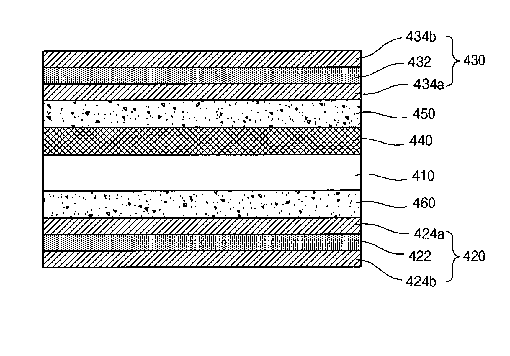
[0062]FIG. 11 is a cross-sectional view schematically illustrating an IPS-LCD device according to the present invention. As shown in FIG. 11, the IPS-LCD device includes a liquid crystal panel 310, a first polarizer 320 at a lower surface of the liquid crystal panel 310, and a second polarizer 330 at an upper surface of the liquid crystal panel 310. First and second optical compensation films 340 and 350 are disposed between the liquid crystal panel 310 and the second polarizer 320.

[0063]Although not shown in the figure, the liquid crystal panel 310 includes first and second substrates and a liquid crystal layer interposed between the first and second substrates. The liquid crystal panel 310 is operated in an in-plane switching mode, in which a thin film transistor, a common electrode and a pixel electrode are formed on an inner surface of the first substrate whereas a black matrix and a color filter layer are formed on an inner surface of the second substrate. An overcoat layer may...


PUM

PropertyMeasurementUnit
thicknessaaaaaaaaaa
azimuthal angleaaaaaaaaaa

Abstract

An in-plane switching liquid crystal display device includes a liquid crystal display panel having first and second substrates, a first polarizer disposed at a first surface of the liquid crystal display panel and having a first protective film, a first polarizing film, and a second protective film, a second polarizer disposed at a second surface of the liquid crystal display panel and having a third protective film, a second polarizing film, and a fourth protective film, and a first optical compensation film between the first polarizer and the liquid crystal display panel, the third protective film being adjacent to the liquid crystal display panel and having a substantially zero retardation value.

Description

[0001]The present invention claims the benefit of Korean Patent Application Nos. 2005-0057876 and 2005-0057901 both filed on Jun. 30, 2005 and 2006-0020037 filed on Mar. 2, 2006, which are hereby incorporated by reference in their entirety.BACKGROUND OF THE INVENTION[0002]1. Field of the Invention[0003]The present invention relates to a liquid crystal display (LCD) device. More particularly, the present invention relates to an in-plane switching liquid crystal display (IPS-LCD) device and a method of fabricating the same.[0004]2. Discussion of the Related Art[0005]In general, a liquid crystal display (LCD) device includes two substrates, which are spaced apart and face each other, and a liquid crystal layer interposed between the two substrates. Electrodes are formed on the both substrates and face each other. A voltage is applied to each of the electrodes, and an electric field is induced between the electrodes. An arrangement of liquid crystal molecules is changed by varying the i...

Claims


Application Information

Patent Timeline
Patent Type & Authority Patents(United States)
IPC IPC(8): G02F1/1335
CPCG02F1/133528G02F1/133634G02F2201/50G02F2001/133638G02F1/134363G02F1/133638
Inventor LEE, JOUN-HOLEE, GI-DONG
Owner LG DISPLAY CO LTD
Why Eureka
Try Eureka