Memory device, data recording method and IC tag

a memory device and data recording technology, applied in the field of memory devices, data recording methods, and ic tags, can solve problems such as difficult cost reduction

Inactive Publication Date: 2011-06-21
UNIVERSITY OF YAMANASHI +1
View PDF17 Cites 2 Cited by
  • Summary
  • Abstract
  • Description
  • Claims
  • Application Information

AI Technical Summary

Benefits of technology

[0009]The present inventors conducted diligent research on further applications of the electroconductive liquid crystal semiconductors and found that a memory cell of a memory device can be provided through a simple process such as coating of a semiconductor solution or vacuum evaporation of the semiconductor material under room temperature conditions, and thus completed the present invention.
[0010]That is, an object of the present invention is to provide a novel memory device, and a data recording method and an IC tag using the memory device, a memory cell of the memory device being able to be produced using an electroconductive liquid crystal semiconductor through a simple process such as coating of the semiconductor solution or vacuum evaporation of the semiconductor material under room temperature conditions.

Problems solved by technology

Production of semiconductor devices using conventional semiconductors necessarily involves high vacuum and high temperature processing operations, which has made cost reduction difficult.

Method used


Image

  • Memory device, data recording method and IC tag
  • Memory device, data recording method and IC tag
  • Memory device, data recording method and IC tag

Examples


production example 1

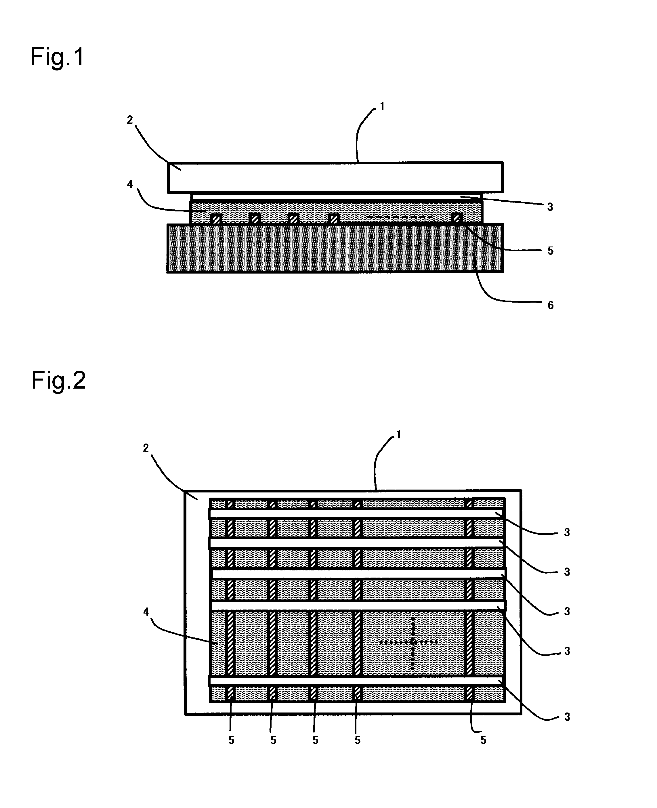
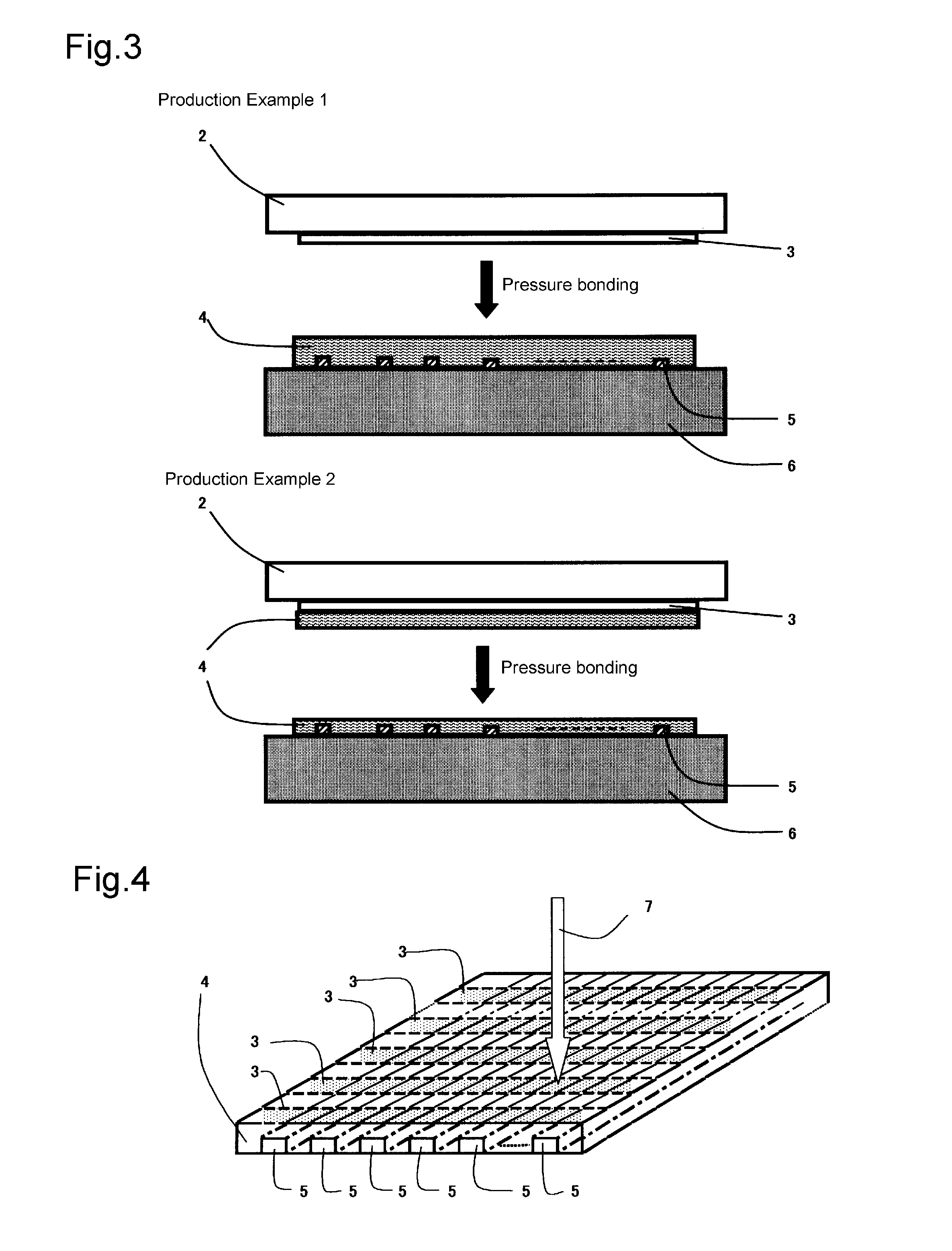
[0075]The first electrode group (5) and the second electrode group (3) containing the transparent electrodes are formed on the lower substrate (6) and on the transparent substrate (2), respectively. Then, on the lower substrate (6) with the electrode group (5) disposed thereon, the layer containing the liquid crystal compound having a smectic phase as the liquid crystal phase is formed to cover the electrode group (5), thus providing the electroconductive liquid crystal semiconductor material layer (4). The lower substrate (6) provided with the electroconductive liquid crystal semiconductor material layer (4) and the transparent substrate (2) provided with an electrode group (3) are pressure bonded. (See Production Example 1, FIG. 3)

production example 2

[0076]The first electrode group (5) and the second electrode group (3) containing transparent electrodes are formed on the lower substrate (6) and on the transparent substrate (2), respectively. Then, the electroconductive liquid crystal semiconductor material layer (4) containing liquid crystals having a smectic phase is formed on the transparent electrodes as a liquid crystal phase. Meanwhile, the electroconductive liquid crystal material layer (4) containing the liquid crystal compound having a smectic phase as a liquid crystal phase is also formed on the lower substrate (6), on which the first electrode group (5) is formed, to cover the electrode group (5). The lower substrate (6) and the transparent substrate (2) thus prepared are pressure bonded on the electroconductive liquid crystal semiconductor material layer (4) (See Production Example 2, FIG. 3).

[0077]As a method to form the electrodes, there may be mentioned a method where an electroconductive thin film formed by vacuum...

synthesis example 1

Styryl Derivative (A)

Synthesis of 1,4-bis(4′-pentadecanoxystyryl)benzene-(E,E)

[0105](1) p-Pentadecanoxybenzaldehyde was prepared by the steps described below in accordance with the following reaction scheme.

[0106]

[0107]In a 100 ml four-necked flask, 2.79 g (42.3 mM) of 85 wt % potassium hydroxide was suspended in 30 ml of dimethylformamide, and 10 ml of a dimethylformamide solution containing 5.28 g (43.2 mM) of hydroxybenzaldehyde was added dropwise while maintaining the system at 20° C. or lower, and the resultant was aged at 30° C. for 1 hour. Next, 9.58 g (32.9 mM) of 1-bromopentadecane was added, and the resultant was aged at 70° C. for 21 hours. The reaction mixture was dispersed in water and extracted with toluene. The extract was washed with water and concentrated to give 11.03 g of a slightly colored viscous liquid. Recrystallization from hexane gave 8.91 g of p-pentadecanoxybenzaldehyde (purity: 98.3%).

[0108](2) A 1,4-bis(4′-pentadecanoxystyryl)benzene isomeric mixture (co...


PUM

PropertyMeasurementUnit
temperatureaaaaaaaaaa

Abstract

A memory device of the present invention is characterized by a memory device for storing information by making use of molecular alignment of a liquid crystal compound in a liquid crystalline state formed by spot irradiation with a laser beam to carry out a selective heat treatment on an electroconductive liquid crystal semiconductor material layer containing a liquid crystal compound, comprising: a first electrode group including a plurality of linear electrodes which are parallel to each other; an electroconductive liquid crystal semiconductor material layer formed in such a manner that the layer covers the first electrode group, the layer containing a liquid crystal compound having a long linear conjugate structural moiety and exhibiting a smectic phase as a liquid crystal phase; and a second electrode group formed on the electroconductive liquid crystal semiconductor material layer and including a plurality of linear transparent electrodes being parallel to each other and extend in a direction intersecting with the first electrode group.

Description

TECHNICAL FIELD[0001]The present invention relates to a memory device, a data recording method, and an IC tag using an electroconductive liquid crystal semiconductor.BACKGROUND ART[0002]Organic semiconductors have been attracting attention as a semiconductor material taking the place of silicon and compound semiconductors. Production of semiconductor devices using conventional semiconductors necessarily involves high vacuum and high temperature processing operations, which has made cost reduction difficult. In contrast, use of organic semiconductor materials will make it feasible to produce semiconductor devices through a simple processing operation such as coating with a semiconductor solution or vacuum evaporation of the semiconductor material under room temperature conditions.[0003]The inventors of the present invention previously found that a liquid crystal compound having a long linear conjugate structure and having a smectic phase as a liquid crystal phase develops excellent c...

Claims


Application Information

Patent Timeline
Patent Type & Authority Patents(United States)
IPC IPC(8): G11C13/04
CPCB82Y10/00G11C13/0014G11C13/0016H01L27/10H01L51/0076H01L51/0026H01L51/0037G11C13/04H10K71/40H10K85/1135H10K85/731H01L27/105
Inventor HARAMOTO, YUICHIROKATO, TAKAMASAHIROSHIMA, KOHKI
Owner UNIVERSITY OF YAMANASHI
Why Eureka
Try Eureka