One-time-programmable anti-fuse formed using damascene process

a damascene process and one-time-programmable technology, applied in the direction of semiconductor devices, semiconductor/solid-state device details, electrical apparatus, etc., can solve the problems of increasing complexity and cost, increasing complexity and cost of fabricating integrated circuits, and not being compatible with current copper damascene processes. achieve the effect of reducing write voltag

Active Publication Date: 2011-06-28
TAIWAN SEMICON MFG CO LTD
View PDF30 Cites 13 Cited by
  • Summary
  • Abstract
  • Description
  • Claims
  • Application Information

AI Technical Summary

Benefits of technology

[0012]The advantageous features of the present invention include reduced write voltages and full compatibility with the existing formation processes of integrated circuits.

Problems solved by technology

Typically, the manufacturing techniques used to form non-volatile memory are quite different from standard logic processes, thereby dramatically increasing the complexity and cost.
Conventional OTP memory devices were typically fabricated using aluminum interconnect technologies, which involve aluminum deposition, patterning, and etching, and thus are not compatible with current copper damascene processes, which have become standard processes.
Such high voltage or high current requirements need to be taken into design considerations, and thus the complexity and the cost of fabricating integrated circuits increases accordingly.

Method used


Image

  • One-time-programmable anti-fuse formed using damascene process
  • One-time-programmable anti-fuse formed using damascene process
  • One-time-programmable anti-fuse formed using damascene process

Examples


first embodiment

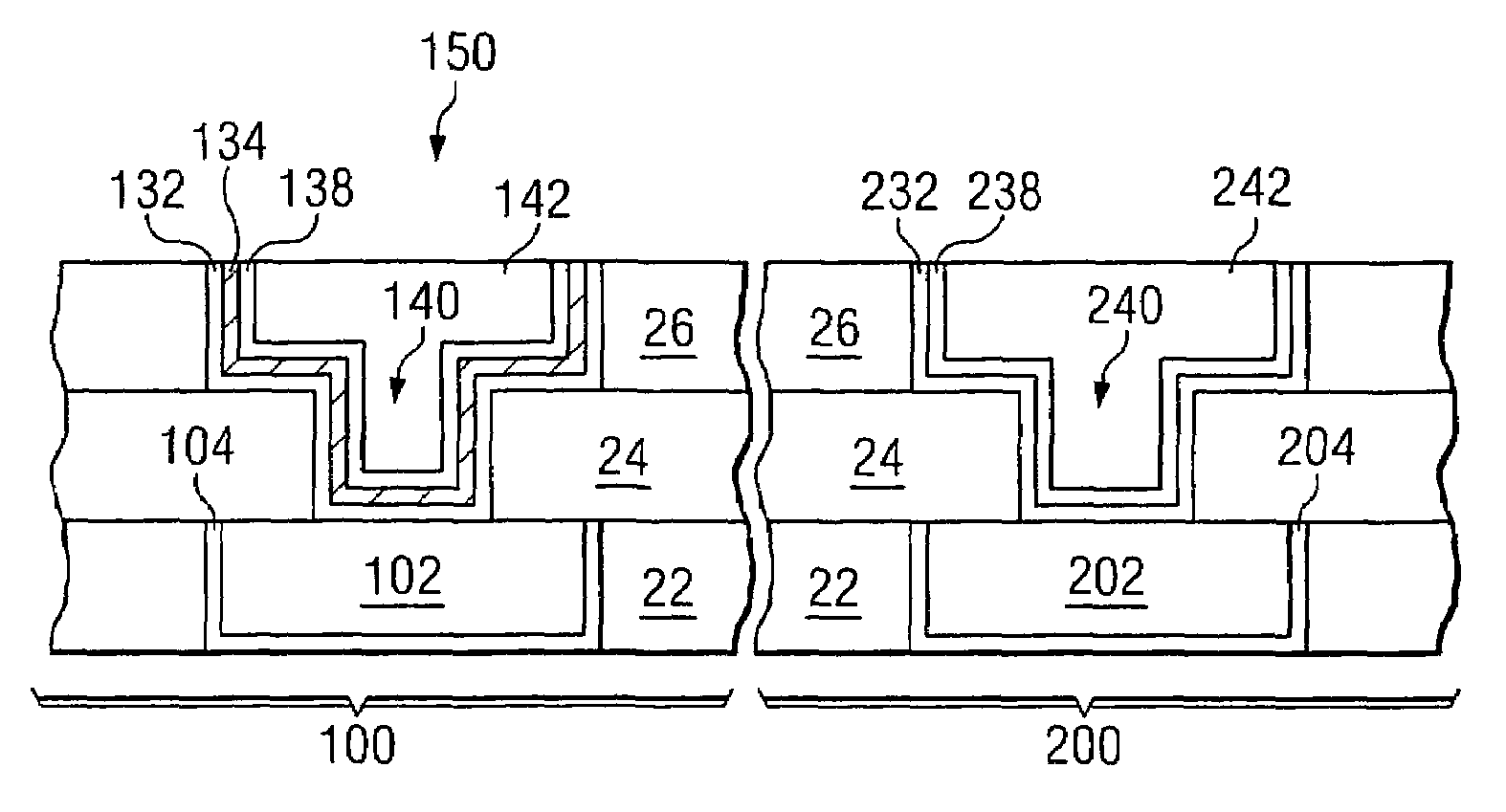
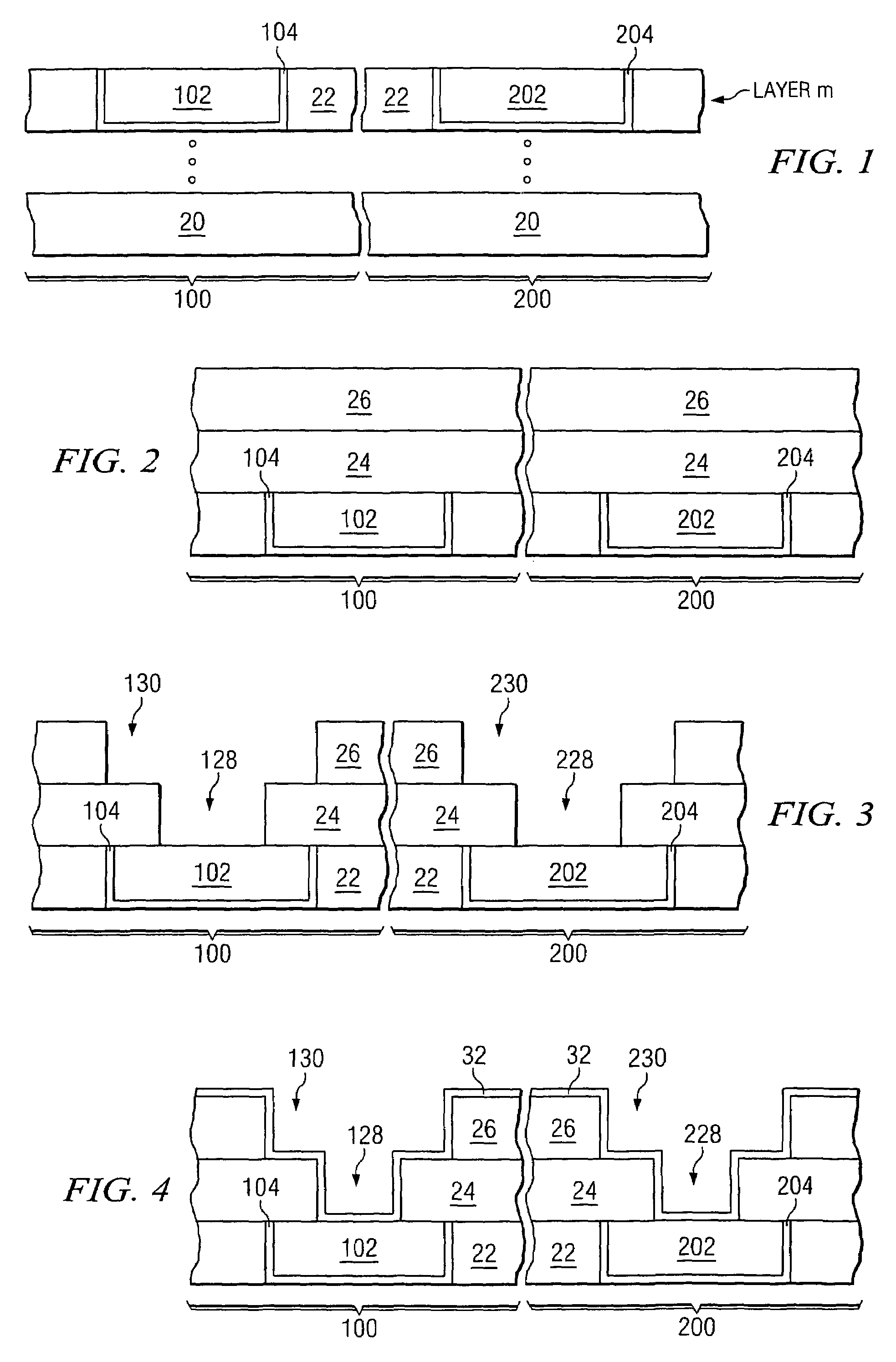
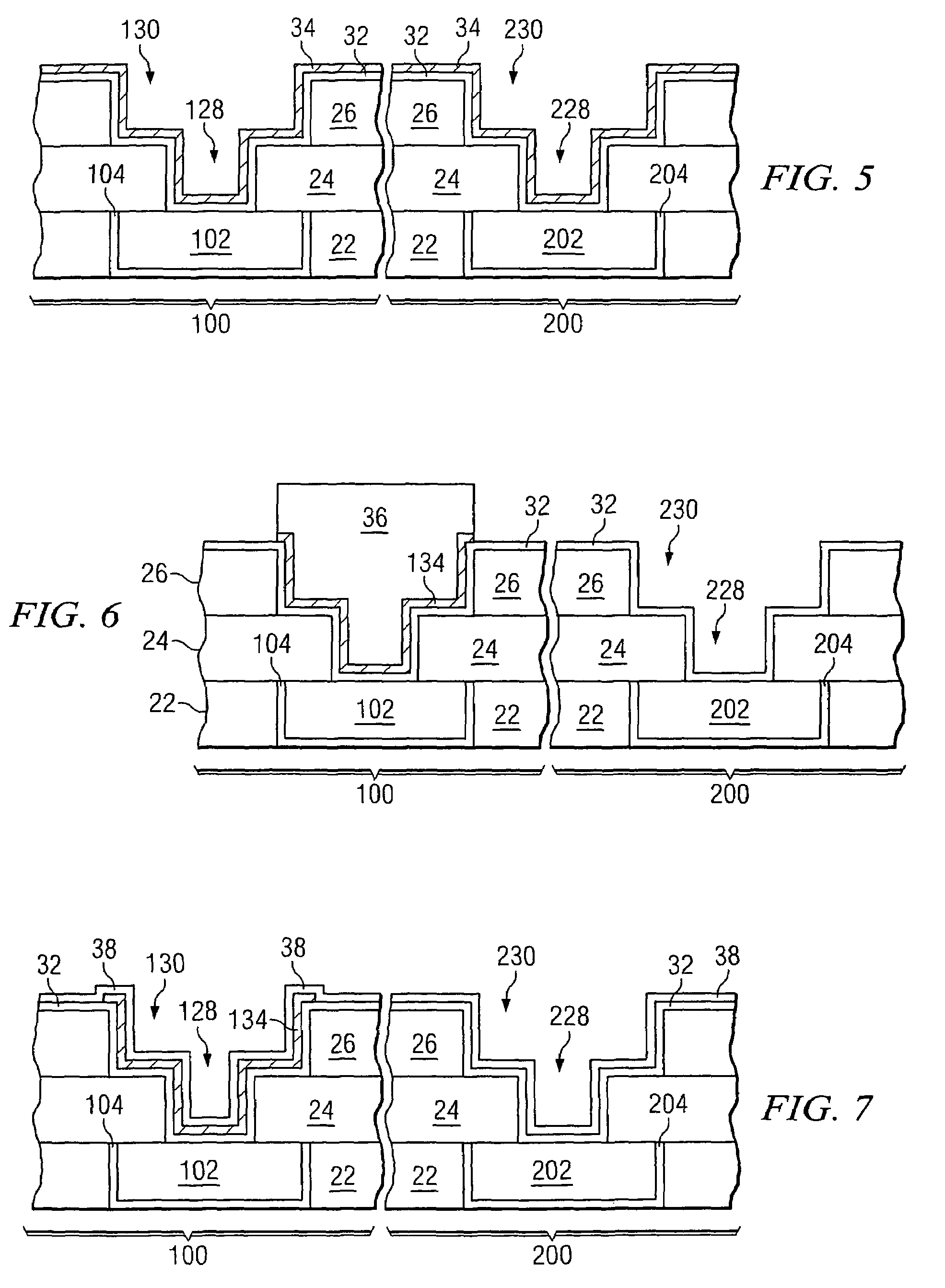
[0025]In a first embodiment, an OTP anti-fuse cell, which has a via-like structure, is formed simultaneously with a via structure. Both the OTP anti-fuse and the via structure comprise lower-level metal lines and upper-level metal lines interconnected by vias. FIG. 1 illustrates two regions 100 and 200 over a semiconductor substrate 20, which have devices (not shown) formed thereon. Region 100 is used for forming an OTP anti-fuse cell, and region 200 is used for forming a via. FIG. 1 also illustrates a metallization layer m over the semiconductor substrate 20, wherein metallization layer m includes a dielectric layer 22, a lower-level metal feature 102 in region 100 and a lower-level metal feature 202 in region 200. Metallization layer m may be any of the metallization layers except the top metallization layer. Dielectric layer 22 preferably comprises a material having a dielectric constant (k value) of less than 3.9, and may contain nitrogen, carbon, hydrogen, oxygen, fluorine, and...

second embodiment

[0041]In a second embodiment, an OTP anti-fuse having a crown-type MIM capacitor structure is formed. Referring to FIG. 10, a semiconductor substrate 310 is provided with an insulation layer 314 formed thereon. A metal line 316, for example, a copper line 316, is formed over insulation layer 314, followed by the deposition of an inter-metal dielectric (IMD) layer 320 over metal line 316. A damascene opening 312 is etched through IMD layer 320, exposing metal line 316.

[0042]Referring to FIG. 11, a first diffusion barrier layer 322 is deposited conformally within the damascene opening 312 and on IMD layer 320. First diffusion barrier layer 322 may comprise titanium nitride, tantalum nitride, titanium silicon nitride, and / or tantalum silicon nitride. A first copper layer 324 is formed over first diffusion barrier layer 322, for example, by electroplating or electroless plating. The copper is formed on the bottom and sidewalls of the damascene opening. First copper layer 324 will form a...

third embodiment

[0046]In the present invention, an OTP anti-fuse having a planar MIM structure, as is shown in FIG. 13, is formed. The planar anti-fuse includes a top plate 412, a bottom plate 414 and an insulation layer 410 therebetween. Bottom plate 414 is preferably bigger than top plate 412. Contact plugs 416 and 418 connect to the bottom plate 414 and top plate 412, respectively. Each of the top and bottom plates 412 and 414 may further include diffusion barrier layers. One skilled in the art will realize the respective formation steps.


PUM


Abstract

A semiconductor structure includes a semiconductor substrate, a power source, and a stacked structure over the semiconductor substrate and coupled to the power source. The stacked structure includes a bottom electrode, a top electrode, and an insulation layer between the top electrode and the bottom electrode, wherein the insulation layer has a breakdown voltage lower than a pre-determined write voltage provided by the power source and higher than a pre-determined read voltage provided by the power source.

Description

TECHNICAL FIELD[0001]This invention relates generally to semiconductor devices, and more particularly to the structure and fabrication methods of one-time-programmable anti-fuse cells.BACKGROUND[0002]In the field of data storage, there are two main types of storage elements. The first type is volatile memory, in which information is stored in a particular storage element and the information is lost the instant the power is removed from the circuit. The second type is a non-volatile storage element, in which the information is preserved even when the power is removed. Of the second type, some designs allow multiple programming while other designs allow only one-time programming. Typically, the manufacturing techniques used to form non-volatile memory are quite different from standard logic processes, thereby dramatically increasing the complexity and cost.[0003]Typically, one-time-programmable (OTP) memory devices include metal fuses, gate oxide fuses, etc. Metal fuses, as the name s...

Claims


Application Information

Patent Timeline
Patent Type & Authority Patents(United States)
IPC IPC(8): H01L23/52H01L23/48H01L29/40
CPCH01L23/5252H01L2924/0002H01L2924/00
Inventor WANG, MING-TSONGONG, TONG-CHERN
Owner TAIWAN SEMICON MFG CO LTD
Why Eureka
Try Eureka