
Memory based on spin texture, and preparation method thereof
A memory and texture technology, applied in the storage field, can solve the problems of inability to further reduce the size, fail to meet high-density integration, and limited information writing speed, and achieve fast information reading speed, low power consumption, and small size Effect
- Summary
- Abstract
- Description
- Claims
- Application Information
AI Technical Summary
Problems solved by technology
Method used
Image

Examples
Embodiment Construction
[0032] The principles and features of the present invention are described below in conjunction with the accompanying drawings, and the examples given are only used to explain the present invention, and are not intended to limit the scope of the present invention.
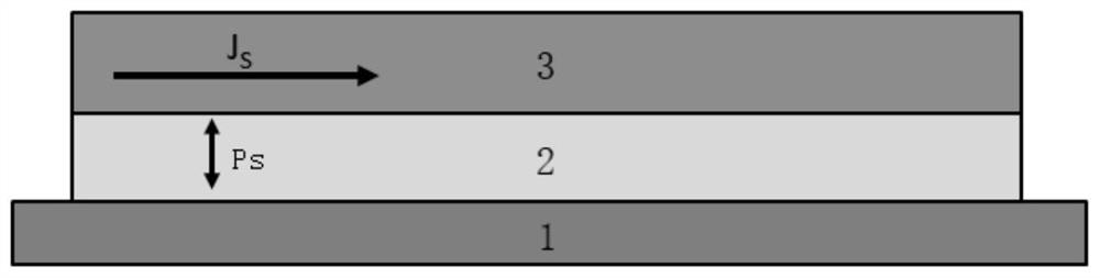
[0033] like figure 1 As shown, a spin texture-based memory provided by an embodiment of the present invention includes a substrate 1, a ferroelectric layer 2 and a ferromagnetic layer 3;
[0034] The ferroelectric layer 2 is located on the substrate 1;
[0035] The ferromagnetic layer 3 is located on the ferroelectric layer 2;
[0036] The material of the substrate 1 is a conductive material, and the material of the ferroelectric layer 2 is GeTe, SnTe or HfO 2 , the material of the ferromagnetic layer 3 is a material that conducts electrons with spin polarization.
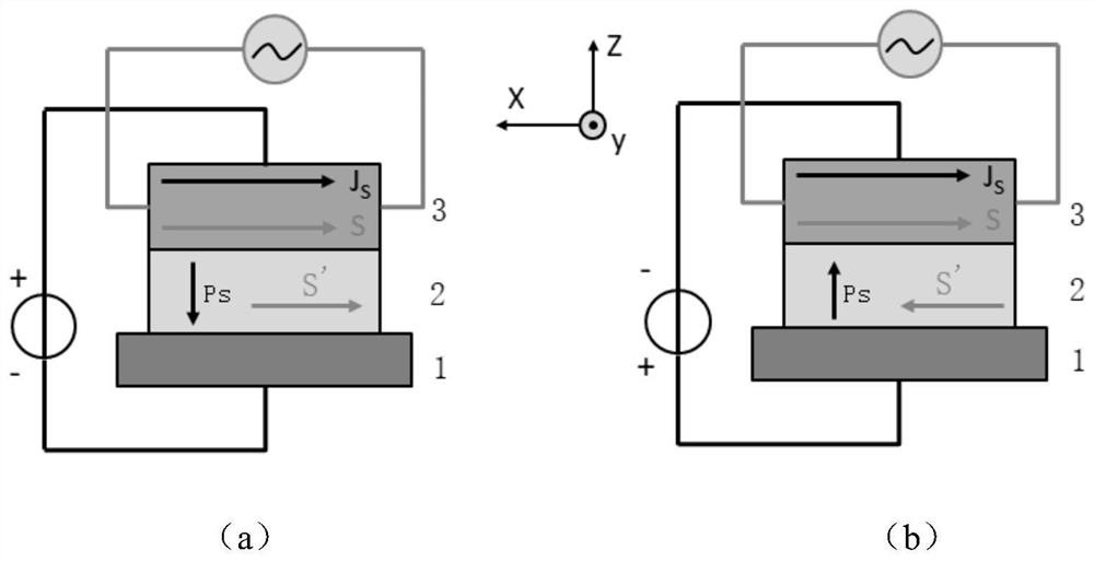
[0037] In the above embodiment, the substrate 1 and the ferromagnetic layer 3 can be used as electrodes to apply an electric field to the ferroelectr...
PUM
| Property | Measurement | Unit |
|---|---|---|
| thickness | aaaaa | aaaaa |
| thickness | aaaaa | aaaaa |
Abstract
Description
Claims
Application Information