

Magnetization rotation element, magnetoresistive effect element, semiconductor element, magnetic recording array, and method for manufacturing magnetoresistive effect element
A technology of magnetoresistance effect elements and rotating elements, which is applied in the manufacture/processing of semiconductor devices, electromagnetic devices, electrical components, etc., which can solve problems such as the degradation of magnetoresistance effect element characteristics, and achieve the effect of reducing the writing voltage
- Summary
- Abstract
- Description
- Claims
- Application Information
AI Technical Summary
Problems solved by technology
Method used
Image

Examples
no. 1 approach
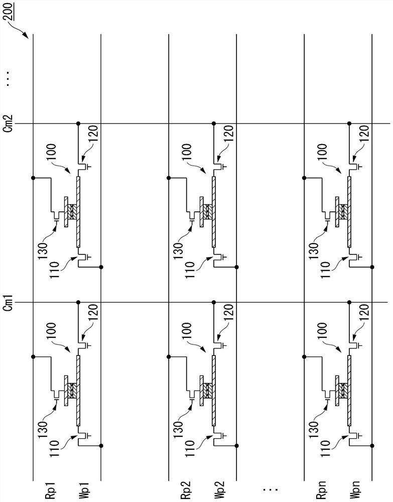
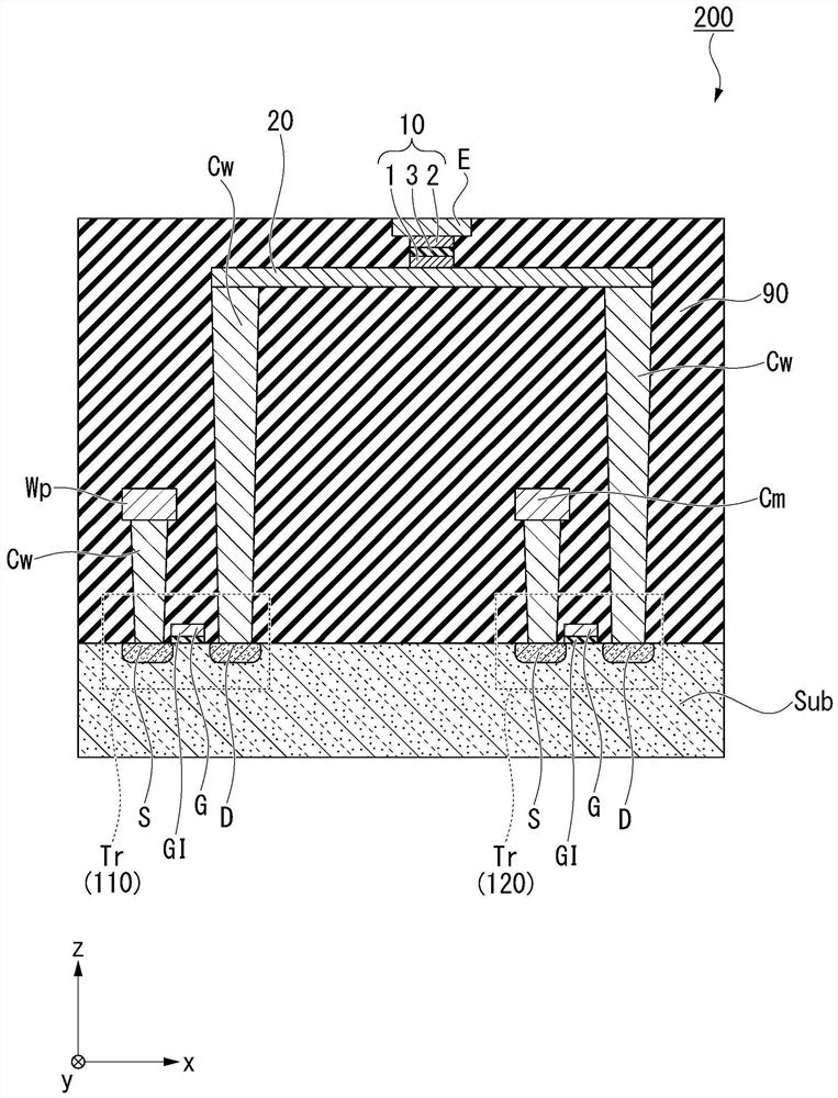
[0064] figure 1 It is a configuration diagram of the magnetic recording array 200 according to the first embodiment. The magnetic recording array 200 includes: a plurality of magnetoresistance effect elements 100 , a plurality of write wirings Wp1 to Wpn, a plurality of common wirings Cm1 to Cmn, a plurality of read wirings Rp1 to Rpn, and a plurality of first switching elements 110 , a plurality of second switching elements 120, and a plurality of third switching elements 130. The magnetic recording array 200 can be used for, for example, a magnetic memory or the like.
[0065] The write wirings Wp1 to Wpn electrically connect a power source to one or more magnetoresistance effect elements 100 . The common lines Cm1 to Cmn are lines used for writing and reading data. The common wirings Cm1 to Cmn electrically connect the reference potential to one or more magnetoresistance effect elements 100 . The reference potential is, for example, ground. The common wirings Cm1 to Cm...
no. 2 approach
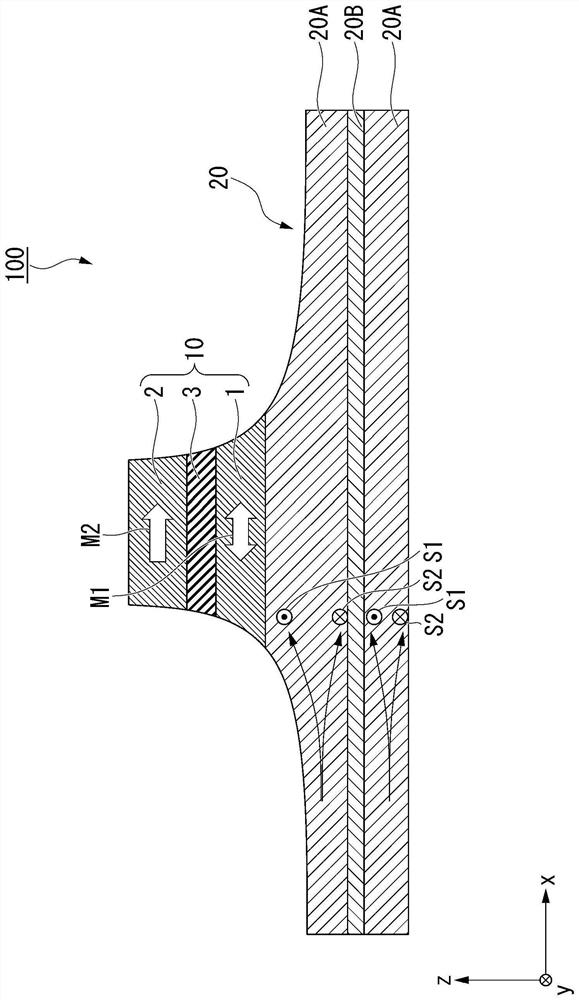
[0142] Figure 15 is a cross-sectional view of the magnetization rotating element 107 according to the second embodiment. Figure 15It is a cross section of the magnetization rotating element 107 cut along the xz plane passing through the center of the width of the spin-orbit torque wiring 20 in the y direction. The magnetization rotating element 107 according to the second embodiment differs from the magnetoresistance effect element 100 according to the first embodiment in that the former does not have the nonmagnetic layer 3 and the second ferromagnetic layer 2 . The rest of the structure is the same as that of the magnetoresistive effect element 100 according to the first embodiment, and description thereof will be omitted.
[0143] The magnetization rotation element 107 makes light L1 incident on the first ferromagnetic layer 1 , and evaluates light L2 reflected by the first ferromagnetic layer 1 . When the orientation direction of the magnetization changes due to the ma...
Embodiment 1
[0149] In Example 1, a spin-orbit torque wiring in which an insertion layer was inserted between spin generation layers was produced. The thickness of the spin-orbit torque wiring was set to 5 nm, and the thickness of the insertion layer was set to 0.2 nm. The spin generating layer of the spin-orbit torque wiring is made of W, and the insertion layer is made of Cu or Ag. Furthermore, CoFeB is laminated on one side of the spin-orbit torque wiring as a first ferromagnetic layer. The first ferromagnetic layer is assumed to be a cylinder with a diameter of 200 nm. By changing the number of insertion layers, the wiring resistance of the spin-orbit torque wiring, the write current required to reverse the magnetization of the first ferromagnetic layer, and the The write voltage required for the magnetization reversal.
[0150] Figure 16 It is a graph showing the wiring resistance of the spin-orbit torque wiring of Example 1. Figure 17 It is a graph showing the write current of...
PUM
| Property | Measurement | Unit |
|---|---|---|
| thickness | aaaaa | aaaaa |
| diameter | aaaaa | aaaaa |
Abstract
Description
Claims
Application Information