Semiconductor device and method of manufacturing the same

a technology of semiconductors and semiconductors, applied in the direction of transistors, coatings, instruments, etc., can solve the problems of tunnel insulating film deterioration, tunnel insulating film breakage, deterioration and breakage, etc., to improve the retention and endurance of non-volatile memory, and reduce the write voltage

Inactive Publication Date: 2019-04-16
ABLIC INC
View PDF11 Cites 0 Cited by
  • Summary
  • Abstract
  • Description
  • Claims
  • Application Information

AI Technical Summary

Benefits of technology

[0022]In view of the foregoing, it is an object of the present invention to provide a non-volatile memory in which retention and endurance are improved through formation of a non-local uneven structure, and a write voltage is decreased.
[0025]The retention and the endurance of the non-volatile memory are improved. Further, the write voltage can be decreased.

Problems solved by technology

With the non-volatile semiconductor memory device in which charge is exchanged through the tunnel insulating film, stress on the tunnel insulating film caused by rewriting between the “0” state and the “1” state as described above deteriorates the tunnel insulating film, and finally causes breakage of the tunnel insulating film.
Further, the deterioration and breakage are greatly associated also with a data storage function of a memory.
Improvement of those characteristics is the most important issue in a memory using the tunnel insulating film.
It is, however, considered to be difficult to improve the endurance by the procedure described in Japanese Patent Application Laid-open No. 2001-135729.
Thus, it is considered to be difficult to improve the endurance and retention with the structure of Japanese Patent Application Laid-open No. 2001-135729.
On the contrary, since the area of the region A of Japanese Patent Application Laid-open No. 2001-135729 is smaller than that of the region A of the related art that does not include the region B, stress applied on the region A per unit area in Japanese Patent Application Laid-open No. 2001-135729 is higher than that of the related art, and hence, in Japanese Patent Application Laid-open No. 2001-135729, there is a high risk in that the endurance and retention are deteriorated.
Accordingly, it is difficult to improve the endurance and retention with the structure having the local uneven structure at the interface between the floating gate and the tunnel insulating film.

Method used


Image

  • Semiconductor device and method of manufacturing the same
  • Semiconductor device and method of manufacturing the same
  • Semiconductor device and method of manufacturing the same

Examples


Embodiment Construction

[0041]Now, embodiments of the present invention are described with reference to the drawings.

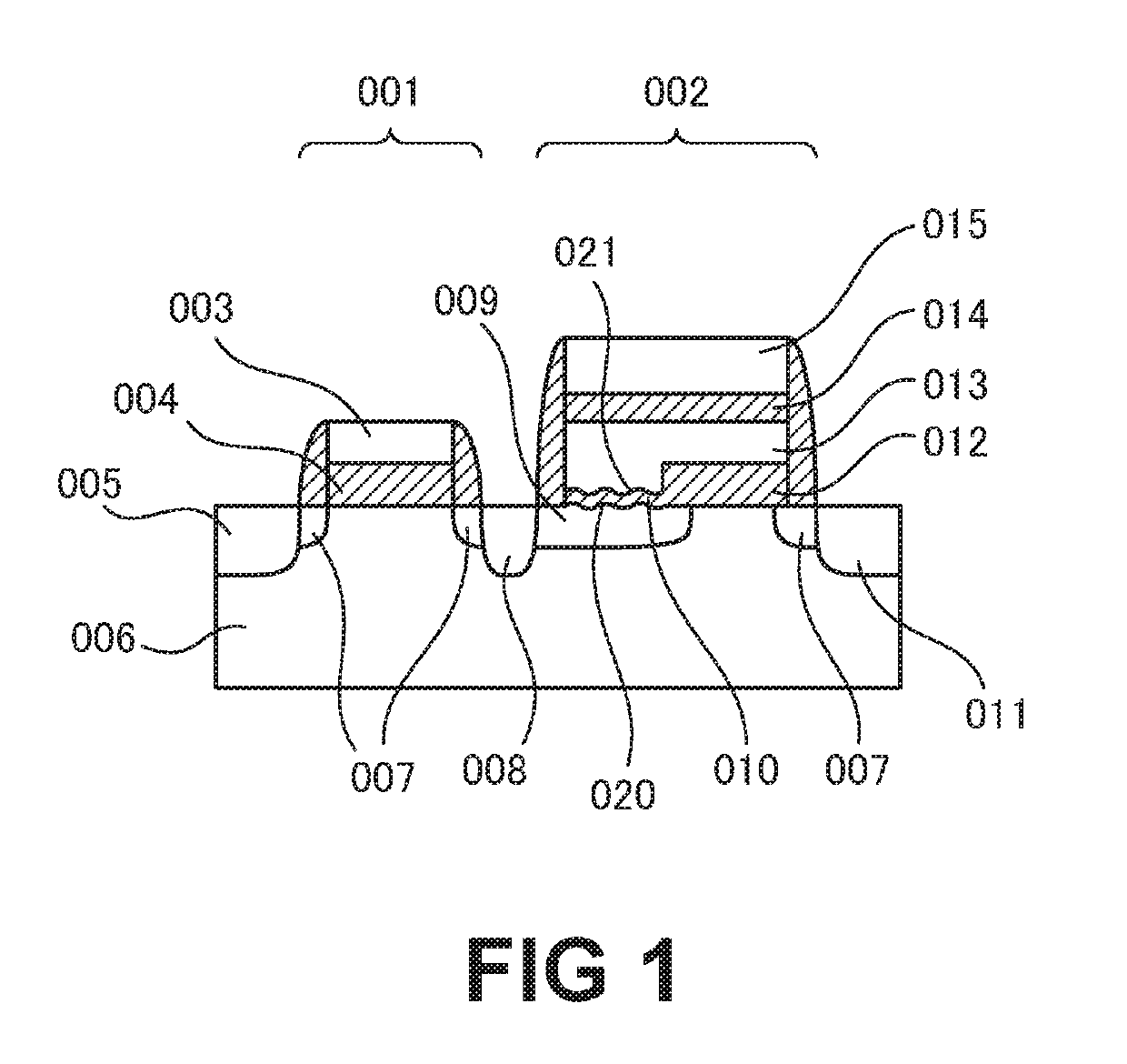
[0042]FIG. 1 is a sectional view for illustrating an EEPROM in an embodiment of the present invention.

[0043]The EEPROM in the embodiment of the present invention includes a memory cell transistor portion 002 and a select gate transistor portion 001 configured to select the memory cell transistor portion 002 in the same manner as in the related-art EEPROM illustrated in FIG. 8.

[0044]The select gate transistor portion 001 includes n-type regions 007 to be source and drain regions formed in a p-type semiconductor substrate 006 or a p-type well region, an n-type select transistor drain region 005 and an n-type select transistor source region 008 formed continuously from the n-type regions 007, a select gate oxide film 004 formed on a surface of the p-type semiconductor substrate 006 or the p-type well region, and a select gate 003 formed on the select gate oxide film 004. In general, the periphe...


PUM

PropertyMeasurementUnit
tunnel insulatingaaaaaaaaaa
insulatingaaaaaaaaaa
lengthaaaaaaaaaa

Abstract

Provided is a semiconductor device which has a non-volatile memory including: a semiconductor substrate; a tunnel insulating film formed on a surface of the semiconductor device; a floating gate formed on the tunnel insulating film; a memory cell transistor drain region and a memory cell transistor source region formed from the surface to an inside of the semiconductor substrate in a vicinity of both ends of the floating gate; a first interface formed between the semiconductor substrate and the tunnel insulating film; and a second interface formed between the floating gate and the tunnel insulating film. The first interface and the second interface form an uneven structure having a curvature that changes at an identical period with respect to a place in sectional view.

Description

RELATED APPLICATIONS[0001]This application claims priority under 35 U.S.C. § 119 to Japanese Patent Application No. 2017-059968 filed on Mar. 24, 2017, the entire content of which is hereby incorporated by reference.BACKGROUND OF THE INVENTION1. Field of the Invention[0002]The present invention relates to a semiconductor device and a method of manufacturing the semiconductor device.2. Description of the Related Art[0003]A related-art non-volatile semiconductor memory device is described by taking an EEPROM as an instance. FIG. 8 is a simplified cross-sectional view for illustrating a memory cell structure of a related-art EEPROM having a general structure which is disclosed, for example, in Japanese Patent Application Laid-open No. 2004-71077.[0004]A memory cell includes a memory cell transistor portion 002 and a select gate transistor portion 001 configured to select the memory cell transistor portion 002. In the memory cell transistor portion 002, an electrode called a floating ga...

Claims


Application Information

Patent Timeline
Patent Type & Authority Patents(United States)
IPC IPC(8): H01L27/115H01L29/788H01L21/283G11C11/34G11C16/04H01L21/822C23C16/24
CPCH01L27/115C23C16/24G11C11/34H01L21/283H01L21/822H01L29/788G11C16/0483G11C16/0433H01L29/40114H10B69/00
Inventor RISAKI, TOMOMITSU
Owner ABLIC INC
Why Eureka
Try Eureka