Memory module with optical interconnect that enables scalable high-bandwidth memory access

a memory module and high-bandwidth technology, applied in the field of memory modules with optical interconnects, can solve the problems of significantly increasing system cost, limiting techniques to short distances, and dominated application performance of memory latency, and achieve the effect of facilitating scalable high-bandwidth memory access

Active Publication Date: 2011-06-28
ORACLE INT CORP
View PDF12 Cites 5 Cited by
  • Summary
  • Abstract
  • Description
  • Claims
  • Application Information

AI Technical Summary

Benefits of technology

One embodiment of the present invention provides a system that facilitates scalable high-bandwidth memory access using a memory module with optical interconnect. This system includes an optical channel, a memory buffer, and a random-access memory module. The memory buffer is configured to receive a request from a memory controller via the optical channel. The memory buffer handles the received request by performing operations on the random-access memory module and then sending a response to the memory controller via the optical channel. Hence, the memory module with optical interconnect provides a high-speed serial link to the random-access memory module without consuming a large number of pins per channel on the memory controller.
In a variation on this embodiment, using an optical channel allows the distance between the memory module and the memory controller to be increased in comparison to other electrical approaches.
In a variation on this embodiment, the memory buffer includes pass-through and merging logic that allows the optical channel to be shared between multiple memory modules with optical interconnect that are coupled in series.
In a further variation, the memory module is configured to use wavelength-division-multiplexing to increase bandwidth and throughput without increasing the number of optical fibers needed. The use of multiple fibers and / or wavelength-division multiplexing allows multiple memory modules with optical interconnect to share the optical channel to provide high-bandwidth memory access.

Problems solved by technology

This growing disparity results from memory suppliers focusing on design objectives based on density and cost rather than on speed.
The growing disparity between processor and memory access speeds is presently causing memory latency to dominate application performance.
However, because each parallel memory channel consumes a large number of pins, simply increasing the number of channels supported by a memory controller can significantly increase system cost.
Fully-buffered memory technology can replace such multi-pin parallel memory channels with high-speed point-to-point serial interfaces, but such techniques are limited to short distances, and the number of connections is still proportional to the number of desired memory channels.

Method used


Image

  • Memory module with optical interconnect that enables scalable high-bandwidth memory access
  • Memory module with optical interconnect that enables scalable high-bandwidth memory access
  • Memory module with optical interconnect that enables scalable high-bandwidth memory access

Examples


Embodiment Construction

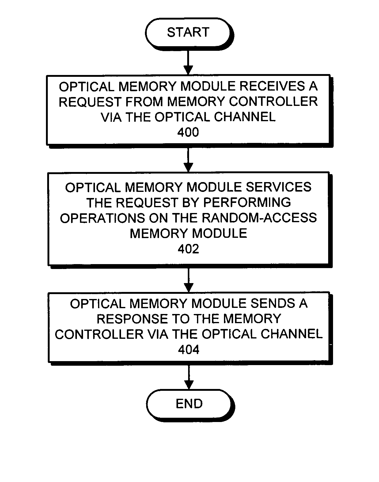
The following description is presented to enable any person skilled in the art to make and use the invention, and is provided in the context of a particular application and its requirements. Various modifications to the disclosed embodiments will be readily apparent to those skilled in the art, and the general principles defined herein may be applied to other embodiments and applications without departing from the spirit and scope of the present invention. Thus, the present invention is not limited to the embodiments shown, but is to be accorded the widest scope consistent with the claims.
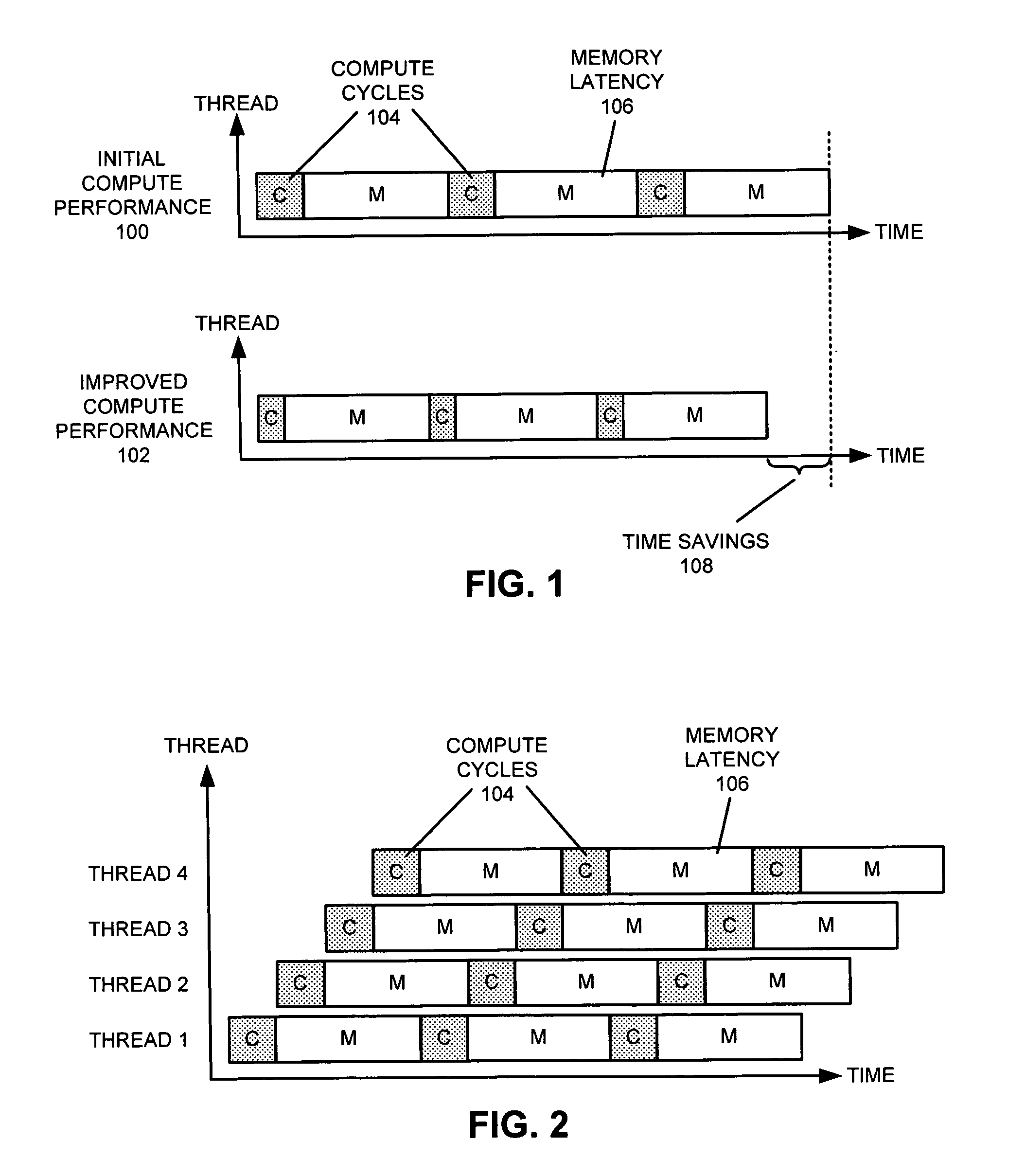
Memory Latency

FIG. 1 illustrates the difficulty of improving system performance purely by improving processor performance without improving memory access speed. The top graph in FIG. 1 shows the initial compute performance 100 of the system based on compute cycles 104 and the memory latency 106 between compute cycles. Dramatically improving the speed of the processor may result in improved compute ...


PUM


Abstract

One embodiment of the present invention provides a system that facilitates scalable high-bandwidth memory access using a memory module with optical interconnect. This system includes an optical channel, a memory buffer, and a random-access memory module. The memory buffer is configured to receive a request from a memory controller via the optical channel. The memory buffer handles the received request by performing operations on the random-access memory module and then sending a response to the memory controller via the optical channel. Hence, the memory module with optical interconnect provides a high-speed serial link to the random-access memory module without consuming a large number of pins per channel on the memory controller.

Description

BACKGROUND1. Field of the InventionThe present invention generally relates to semiconductor memory modules. More specifically, the present invention relates to structures and methods associated with an memory module with optical interconnect that enables scalable high-bandwidth memory access.2. Related ArtA widely-accepted tenet of Moore's Law states that the number of transistors that fit in a square inch of integrated circuitry approximately doubles every two years. For over three decades, technological advances have kept pace with Moore's Law and in doing so have helped to drive processor performance to new heights. Processor manufacturers have exploited the additional circuitry made possible by these advances to build complex processors that support increasing clock frequencies and instruction-level parallelism. Today, such processors accelerate a single instruction pipeline by employing multi-gigahertz frequencies and a variety of sophisticated mechanisms and techniques, such a...

Claims


Application Information

Patent Timeline
Patent Type & Authority Patents(United States)
IPC IPC(8): G06F12/00
CPCG11C5/04G11C7/10G11C7/1081G11C7/1054G11C7/1078G11C7/1051
Inventor FORREST, CRAIG S.KRISHNAMOORTHY, ASHOK V.
Owner ORACLE INT CORP
Why Eureka
Try Eureka