Device for producing metal sample and process for producing metal sample

a technology for metal samples and metal samples, applied in the direction of molten metal supply equipment, instruments, manufacturing tools, etc., can solve the problems of inability to control the content of impurities with high accuracy, unable to uniformly disperse impurities in samples, and unable to achieve high accuracy, easy and rapid collection, and high accuracy

Inactive Publication Date: 2011-07-05
PANASONIC CORP
View PDF7 Cites 0 Cited by
  • Summary
  • Abstract
  • Description
  • Claims
  • Application Information

AI Technical Summary

Benefits of technology

[0026]The present invention solves the aforementioned previous problems, and an object thereof is to provide a process and a device for easily and rapidly producing a sample for analysis for determining the content of impurities contained in a molten metal, particularly a molten solder with high accuracy, by energy dispersive fluorescent X-ray analysis.
[0028]The present essential feature enables to immerse a mold in a molten metal, collect a molten metal into a thin sample collection space, and rapidly cool the molten metal to produce a thin metal sample.
[0030]According to the device and the process for collecting a sample for analysis for determining the content of impurities contained in a solder easily, rapidly and with high accuracy of the present invention, a solder sample for energy dispersive fluorescent X-ray analysis can be easily and rapidly collected, and whether four certain hazardous chemical substances (lead, mercury, cadmium, hexavalent chromium) designated by RoHS Directive are contained as impurities or not can be measured with high accuracy.

Problems solved by technology

However, although the previous process for producing a solder sample can easily and rapidly produce a sample, since a shape and a thickness of a sample are irregular, a solidification rate of a solder sample does not partially become constant, impurities are separated into impurities gathering at a rapid solidification rate place and impurities gathering at a slow solidification rate place, and impurities can not be uniformly dispersed in a sample.
As a result, a measurement error of 300 to 800 ppm is generated depending on a measurement location, at determination of the content of impurities.
Therefore, the previous process has a problem that it is not suitable for controlling the impurities content with high accuracy in order to respond to RoHS Directive which restricts the impurities content at not higher than 1000 ppm.

Method used


Image

  • Device for producing metal sample and process for producing metal sample
  • Device for producing metal sample and process for producing metal sample
  • Device for producing metal sample and process for producing metal sample

Examples


Embodiment Construction

[0056]Preferred embodiments of the invention will be explained below with reference to the drawings.

(Aspect 1)

A. Device for Producing Solder Sample from Molten Solder

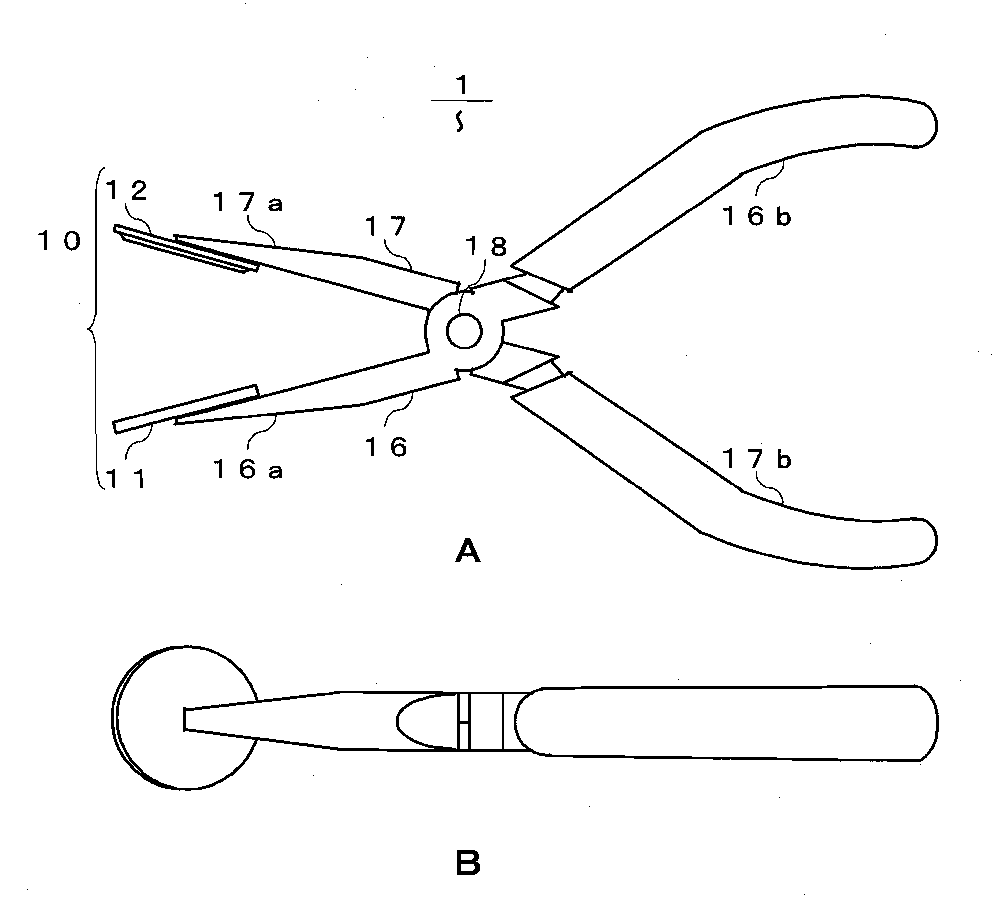
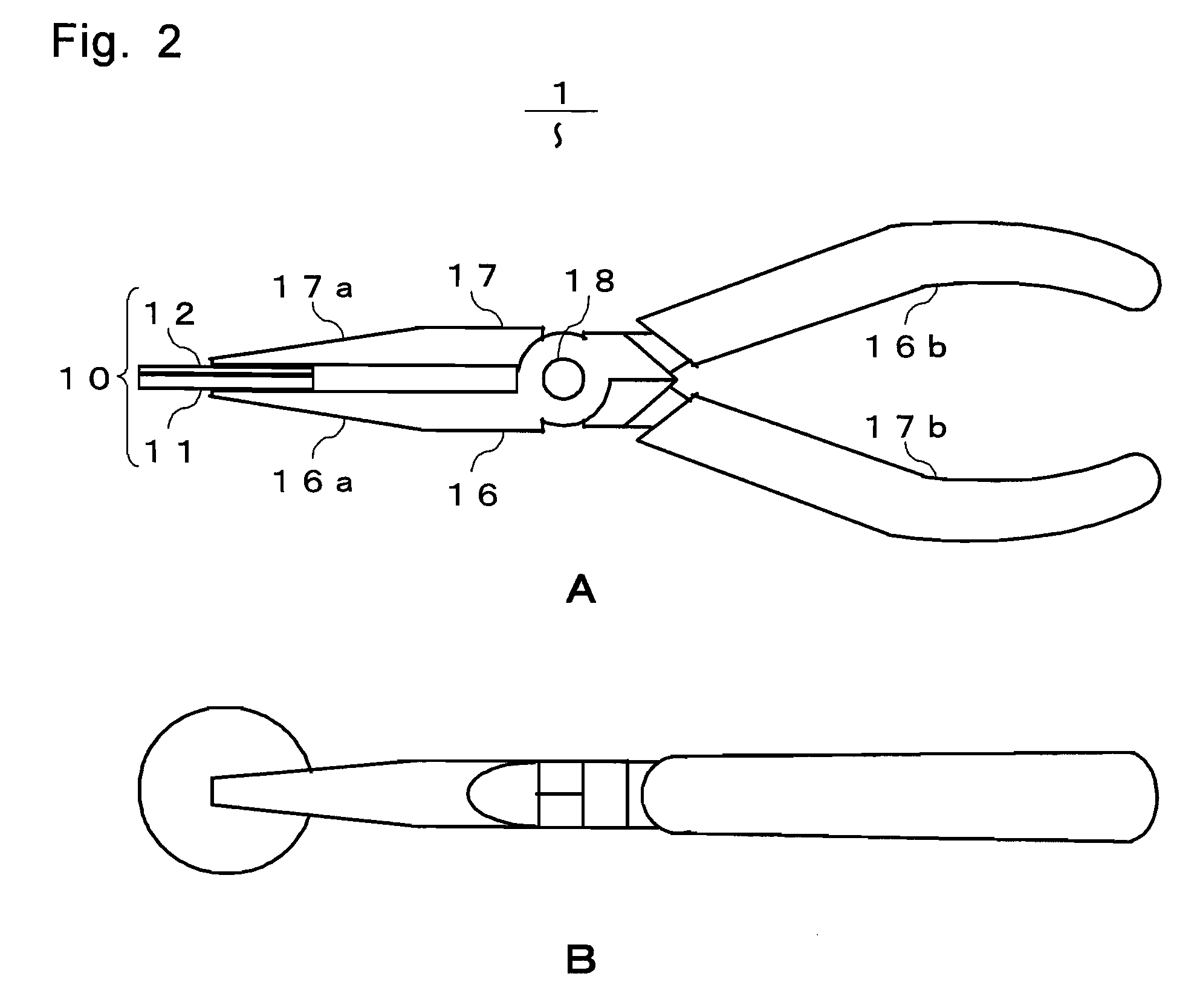
[0057]FIG. 1 and FIG. 2 are a fundamental structural view of a sample production device 1 in accordance with an aspect 1 of the present invention. The sample production device of FIG. 1 consists of a mold 10 which is separated into a lower mold 11 and an upper mold 12, a rotation arm 16 having a rotation arm transmission part 16a and a rotation arm acting force inputting part 16b, which fix and support the lower mold 11, and a rotation arm 17 having a rotation arm transmission part 17a and a rotation arm acting force inputting part 17b, which fix and support the upper mold 12, as an opening / closing operation part with which the mold 10 is opened / closed, and a rotation supporting point 18 which is to be a rotation center for the rotation arm 16 and the rotation arm 17.

[0058]FIG. 1 shows the state where the mold 10 is ope...


PUM

PropertyMeasurementUnit
thicknessaaaaaaaaaa
thicknessaaaaaaaaaa
thicknessaaaaaaaaaa

Abstract

A process and a device for easily and rapidly producing a metal sample for analysis for determining the content of impurities in a molten metal with high accuracy. More particularly, according to the metal sample production process, a metal sample for high accuracy analysis is produced by solidifying a collected molten metal without segregating impurities contained in a molten metal, by rapidly cooling a collected molten metal using a metal sample production device having a thin-walled mold having a thin sample collection space for collecting a molten metal, and an opening / closing operation part with which the mold can be freely opened / closed.

Description

BACKGROUND OF THE INVENTION[0001]1. Technical Field[0002]The present invention relates to a device and a process for collecting a sample for analysis to be used for determining the content of impurities in a metal, particularly a solder easily, rapidly and with high accuracy.[0003]2. Description of the Related Art[0004]Previously, as one of methods of connecting an electronic part to a substrate in manufacturing an electronic circuit substrate, a flow soldering method of using a molten solder material in a form of a jet has been known. This flow soldering method includes generally a flux coating step of coating a substrate with a flux, a pre-heating step of heating the substrate in advance, and a solder material supplying step of contacting the substrate with a jet consisting of a solder material to supply the solder material to the substrate. The previous general flow soldering method will be explained with reference to drawings below. FIG. 22 is a schematic cross-sectional view of...

Claims


Application Information

Patent Timeline
Patent Type & Authority Patents(United States)
IPC IPC(8): B22D46/00G01N1/12
CPCG01N1/125
Inventor KAWASHIMA, YASUJI
Owner PANASONIC CORP
Why Eureka
Try Eureka