ESD protection device

a protection device and electrostatic discharge technology, applied in emergency protective circuit arrangements, transistors, etc., can solve problems such as abnormal operation of electronic products, damage to most electronic devices or systems, and function of integrated circuits, and achieve the effect of improving esd performan

Active Publication Date: 2011-07-12
UNITED MICROELECTRONICS CORP
View PDF3 Cites 5 Cited by
  • Summary
  • Abstract
  • Description
  • Claims
  • Application Information

AI Technical Summary

Benefits of technology

[0006]Accordingly, the present invention is directed to an ESD protection device with enhanced ESD performance.
[0021]As mentioned above, the ESD protection device in the present invention utilizes bipolar junction transistors (BJTs) to achieve ESD protection, and therefore, the parasitic BJT can turn on to bypass the ESD current. Hence, the ESD performance can be improved effectively without compromising the layout area of the ESD protection device.

Problems solved by technology

ESD is the main factor of electrical overstress (EOS) which causes damage to most of electronic devices or systems.
Such damage can result in the permanent damage of semiconductor devices and computer systems, so that the circuit function of integrated circuits (ICs) is affected and the operation of electronic products is abnormal.
In a deep submicron semiconductor process, the ESD tolerance is getting worse as dimensions of the IC devices are getting miniaturized.

Method used


Image

  • ESD protection device
  • ESD protection device
  • ESD protection device

Examples


first embodiment

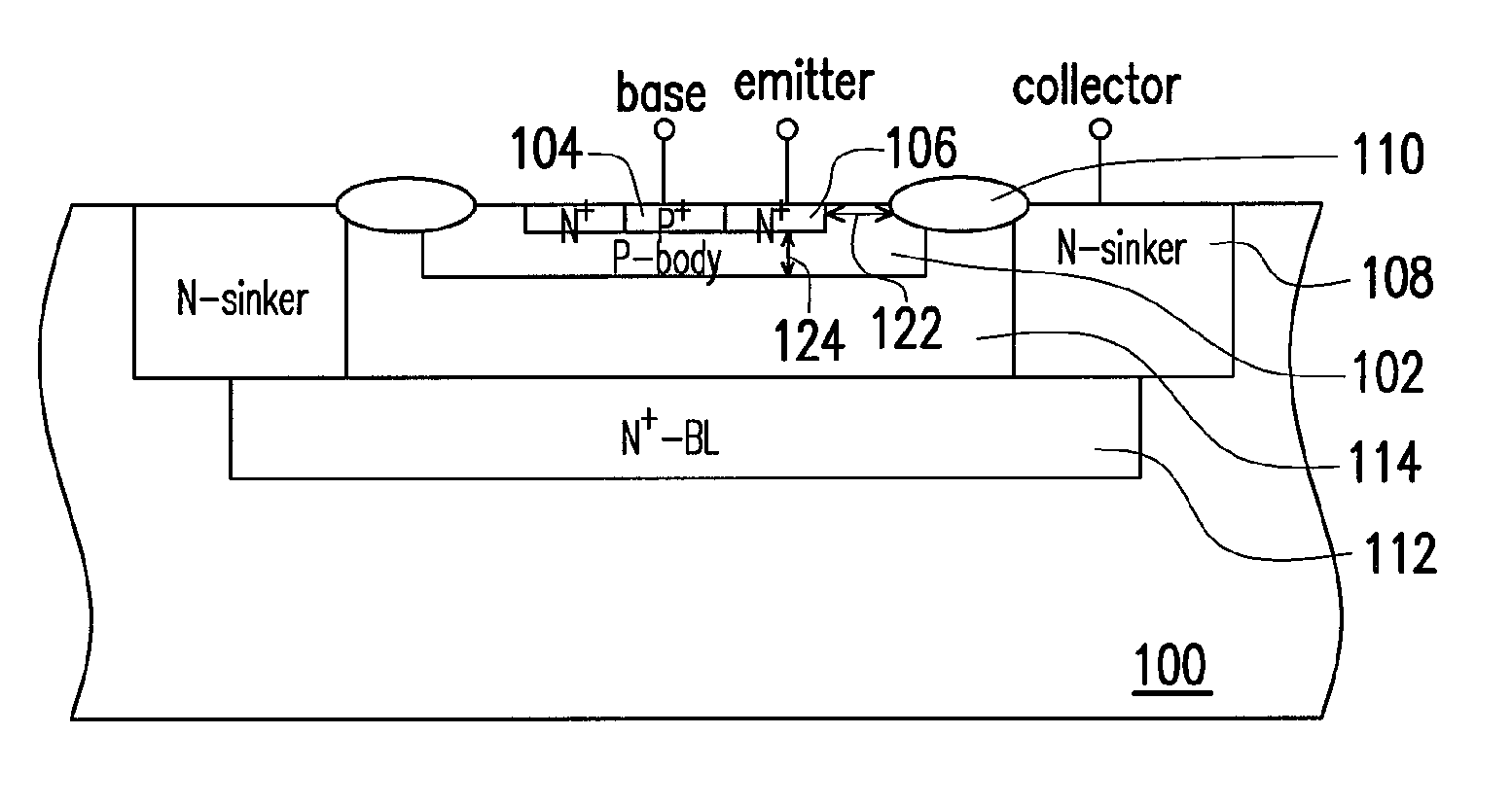
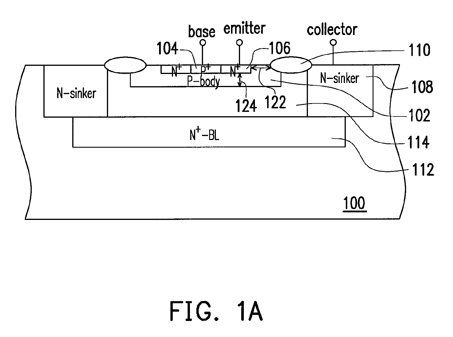
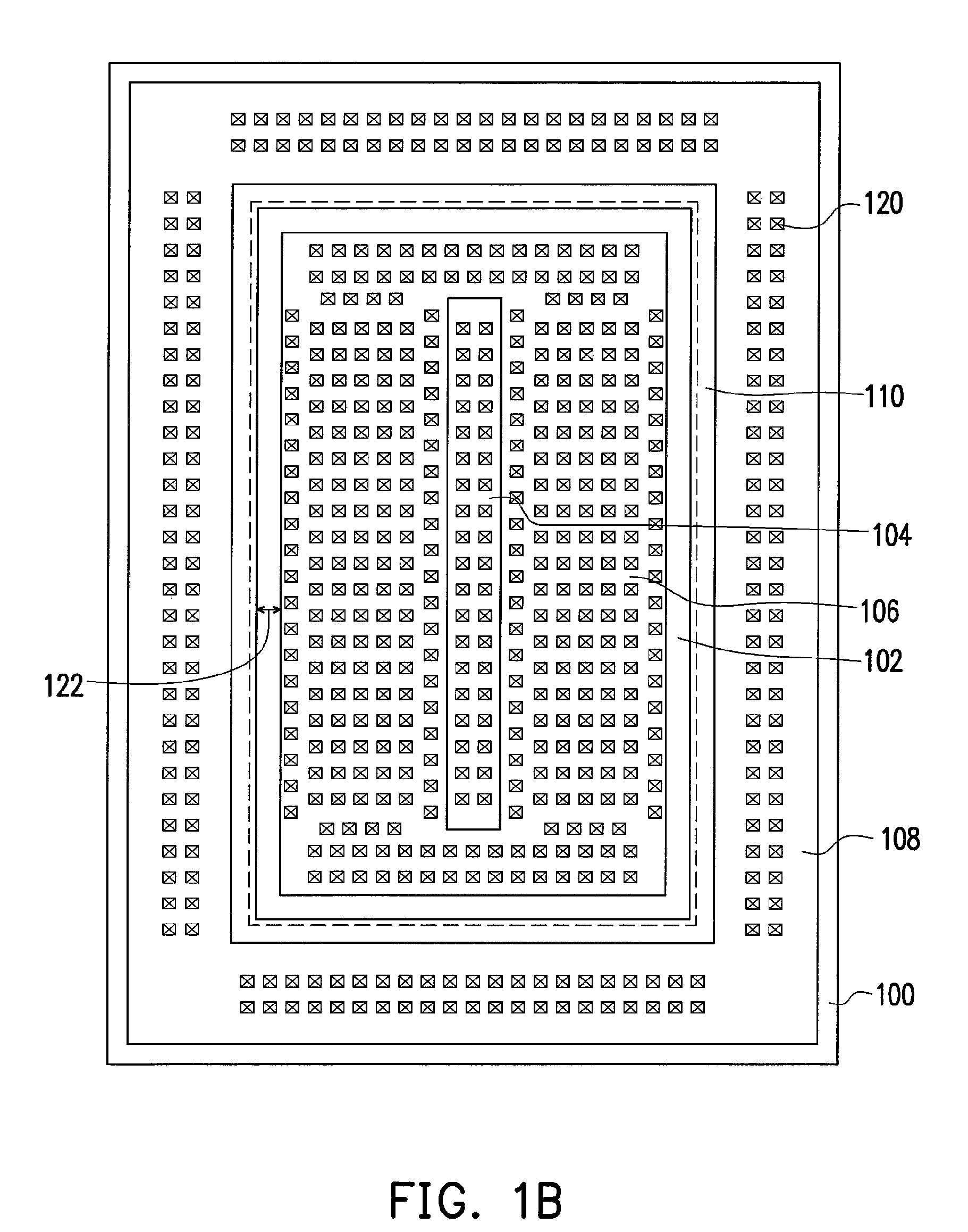
[0034]Referring concurrently to FIGS. 1A and 1B, the ESD protection device of the first embodiment is deployed in a substrate 100. The substrate 100 is, for example, a P-type substrate, and an N-epitaxial layer 114 may be configured therein. The ESD protection device includes a P-body region 102, a P-type doped region 104, an N-type doped region 106, an N-sinker region 108, an N-buried layer 112 and an isolation structure 110.

[0035]The P-body region 102 is configured in the substrate 100 within the N-epitaxial layer 114. The P-type doped region 104, such as a P+ doped region, is configured in the P-body region 102. The P-type doped region 104 can be deployed in the middle of the P-body region 102. The N-type doped region 106, such as an N+ doped region, is configured in the P-body region 102 and surrounds the P-type doped region 104. The N-type doped region 106 may adjoin the profile of the P-type doped region 104. The P-type doped region 104 and the N-type doped region 106, for exa...

second embodiment

[0048]Alternatively, the ESD protection device can be further modified so as to apply to other semiconductor processes. FIG. 4 depicts schematically, in a cross-sectional diagram, the ESD protection device according to the present invention.

[0049]Referring to FIG. 4, the ESD protection device of the second embodiment is deployed in a substrate 400, such as a P-type substrate or a deep N-well region. The ESD protection device includes a first P-type doped region 402, a second P-type doped region 404, a first N-type doped region 406, a second N-type doped region 408 and an isolation structure 410.

[0050]The first P-type doped region 402 is configured in the substrate 400. The second P-type doped region 404, such as a P+ doped region, is configured in the first P-type doped region 402. The second P-type doped region 404 can be deployed in the middle of the first P-type doped region 402. The first N-type doped region 406, such as an N+ doped region, is configured in the first P-type dope...


PUM


Abstract

An ESD protection device is described, which includes a first P-type doped region, a second P-type doped region, a first N-type doped region, a second N-type doped region and an isolation structure. The first P-type doped region is configured in a substrate. The second P-type doped region is configured in the first P-type doped region. The first N-type doped region is configured in the first P-type doped region and surrounds the second P-type doped region. The second N-type doped region is configured in the substrate and surrounds the first P-type doped region. The isolation structure is disposed between the first P-type doped region and the second N-type doped region, wherein a spacing is deployed between an outward edge of the first N-type doped region and the isolation structure.

Description

BACKGROUND OF THE INVENTION[0001]1. Field of the Invention[0002]The present invention relates to a semiconductor device, and in particular, to an electrostatic discharge (ESD) protection device.[0003]2. Description of Related Art[0004]ESD is the main factor of electrical overstress (EOS) which causes damage to most of electronic devices or systems. Such damage can result in the permanent damage of semiconductor devices and computer systems, so that the circuit function of integrated circuits (ICs) is affected and the operation of electronic products is abnormal. Accordingly, a number of methods have been developed to protect the semiconductor IC devices against possible ESD damages. The most common type of ESD protection is the incorporation of a specific hardware inside the IC package. A specially-designed ESD protection device set up between an input pad and an internal device is utmostly required, so as to protect the internal device.[0005]In a deep submicron semiconductor proces...

Claims


Application Information

Patent Timeline
Patent Type & Authority Patents(United States)
IPC IPC(8): H01L29/66
CPCH01L27/0259H01L29/0692H01L29/735
Inventor CHAO, FANG-MEI
Owner UNITED MICROELECTRONICS CORP
Why Eureka
Try Eureka