

Illuminator for a photolithography device
a photolithography and illumination technology, applied in the field of illumination for a photolithography device, can solve the problems of complex and expensive production of illumination according to the prior art, the complexity of such a group is both optical and mechanical, and the complexity of such a group is both complex and expensiv
- Summary
- Abstract
- Description
- Claims
- Application Information
AI Technical Summary
Benefits of technology
Problems solved by technology
Method used
Image

Examples
Embodiment Construction
[0032]The invention is intended to overcome at least one of these disadvantages.
[0033]To this end, the invention proposes an illuminator according to claim 1.
[0034]The invention is advantageously complemented with the features presented in the dependent claims.
[0035]The invention also relates to a device comprising such an illuminator.
[0036]The invention has numerous advantages.
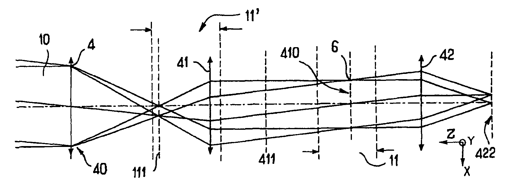
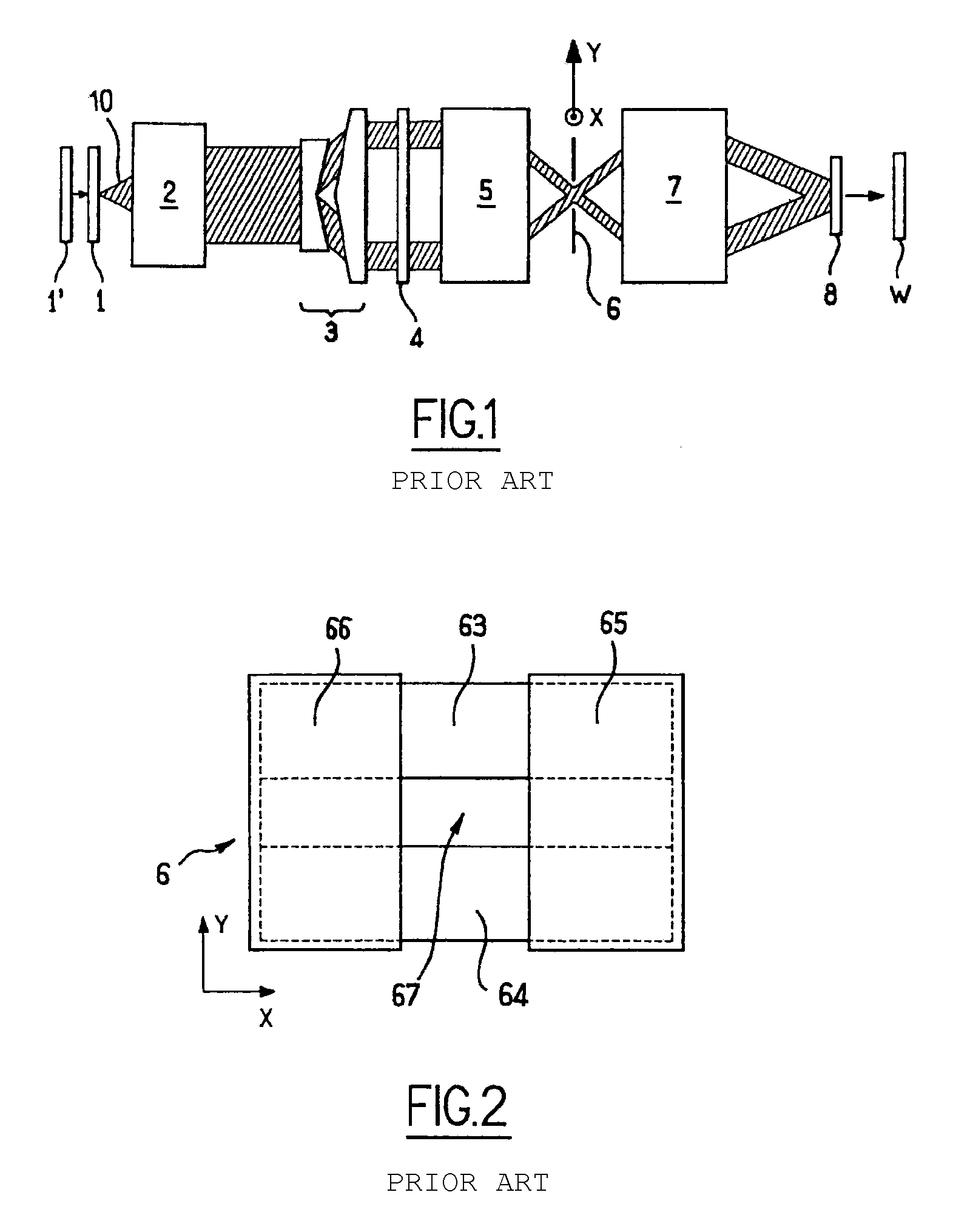
[0037]First, an illuminator according to the invention is simpler and therefore less expensive, due to the absence of a group forming an optical relay in order to conjugate the plane of the shutter and the mask.
[0038]In addition, the mechanical elements enabling the movement of the mobile plates, one with respect to another, are also simpler and therefore less expensive, due to the reduction in amplitude of the course and the speed of translation of the plates. One may expect a reduction by a factor of 10 in the speed of movement of the plates of the shutter, which allows for a reduction in vibrations produce...
PUM
 Abstract
Description
Claims
Application Information