Method for increasing the speed of a light emitting biopolar transistor device

a biopolar transistor and light-emitting technology, applied in the direction of semiconductor devices, basic electric elements, electrical equipment, etc., can solve the problem of fundamental limitation of the speed of bipolar transistors, spontaneous emission recombination lifetime, etc., to enhance stimulated emission, reduce recombination lifetime, and enhance the effect of transistor speed

Active Publication Date: 2011-08-16
THE BOARD OF TRUSTEES OF THE UNIV OF ILLINOIS
View PDF24 Cites 23 Cited by
  • Summary
  • Abstract
  • Description
  • Claims
  • Application Information

AI Technical Summary

Benefits of technology

[0008]Another aspect of the invention involves employing stimulated emission to advantage in the base layer of a bipolar transistor (e.g. a bipolar junction transistor (BJT) or a heterojunction bipolar transistor (HBT), in order to enhance the speed of the transistor. Spontaneous emission recombination lifetime is a fundamental limitation of bipolar transistor speed. In a form of the present invention, the base layer of a bipolar transistor is adapted to enhance stimulated emission (or stimulated recombination) to the detriment of spontaneous emission, thereby reducing recombination lifetime and increasing transistor speed. In a form of this aspect of the invention, at least one layer exhibiting quantum size effects, preferably a quantum well or a layer of quantum dots, preferably undoped or lightly doped, is provided in the base layer of a bipolar transistor. Preferably, at least a portion of the base layer containing the at least one layer exhibiting quantum size effects, is highly doped, and of a wider bandgap material than said at least one layer. The at least one quantum well, or layer of quantum dots, within the higher gap highly doped material, enhances stimulated recombination and reduces radiative recombination lifetime. A two-dimensional electron gas (“2-DEG”) enhances carrier concentration in the quantum well or quantum dot layer, thereby improving mobility in the base region. Improvement in base resistance permits reduction in base thickness, with attendant reduction of base transport time. These advantages in speed are applicable in high speed bipolar transistors in which light emission is utilized, and / or in high speed bipolar transistors in which light emission is not utilized. In light emitting bipolar transistor devices, for example heterojunction bipolar transistors of direct bandgap materials, the use of one or more layers exhibiting quantum size effects can also be advantageous in enhancing light emission and customizing the emission wavelength characteristics of the devices.
[0013]In accordance with another embodiment of the invention, a method is set forth for increasing the speed of a bipolar transistor, including the following steps: providing a bipolar transistor having emitter, base, and collector regions; providing electrodes for coupling electrical signals with the emitter, base, and collector regions; and adapting the base region to enhance stimulated emission to the detriment of spontaneous emission, so as to reduce carrier recombination lifetime in the base region. In a form of this embodiment, the step of adapting the base region to enhance stimulated emission to the deteriment of spontaneous emission comprises providing, in the base region, at least one layer exhibiting quantum size effects, preferably a quantum well(s) and / or a layer(s) of quantum dots, preferably undoped or lightly doped.

Problems solved by technology

Spontaneous emission recombination lifetime is a fundamental limitation of bipolar transistor speed.

Method used


Image

  • Method for increasing the speed of a light emitting biopolar transistor device
  • Method for increasing the speed of a light emitting biopolar transistor device
  • Method for increasing the speed of a light emitting biopolar transistor device

Examples


Embodiment Construction

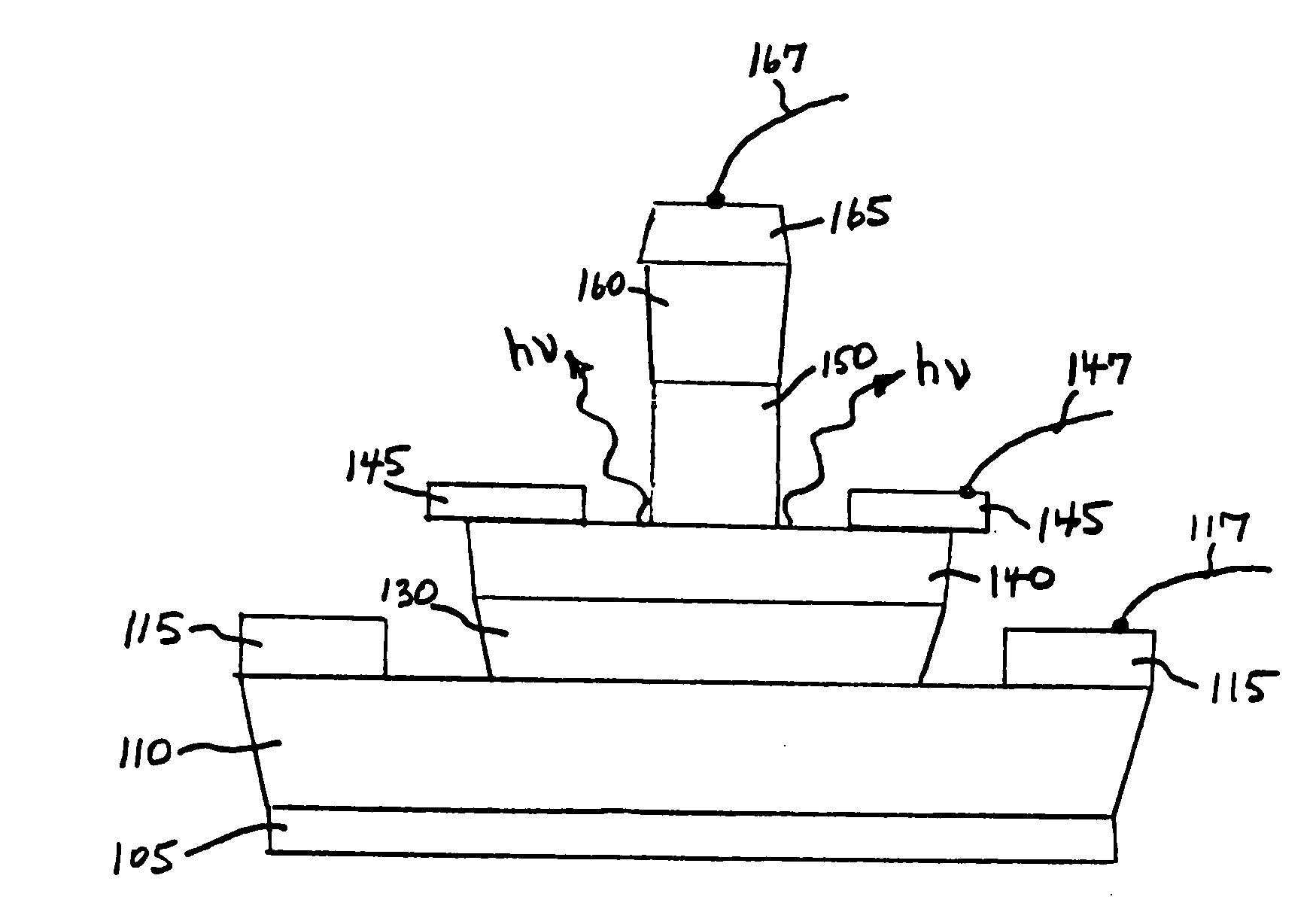
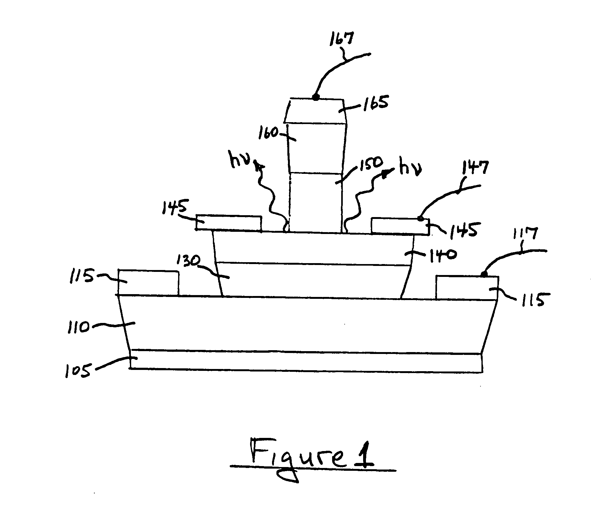
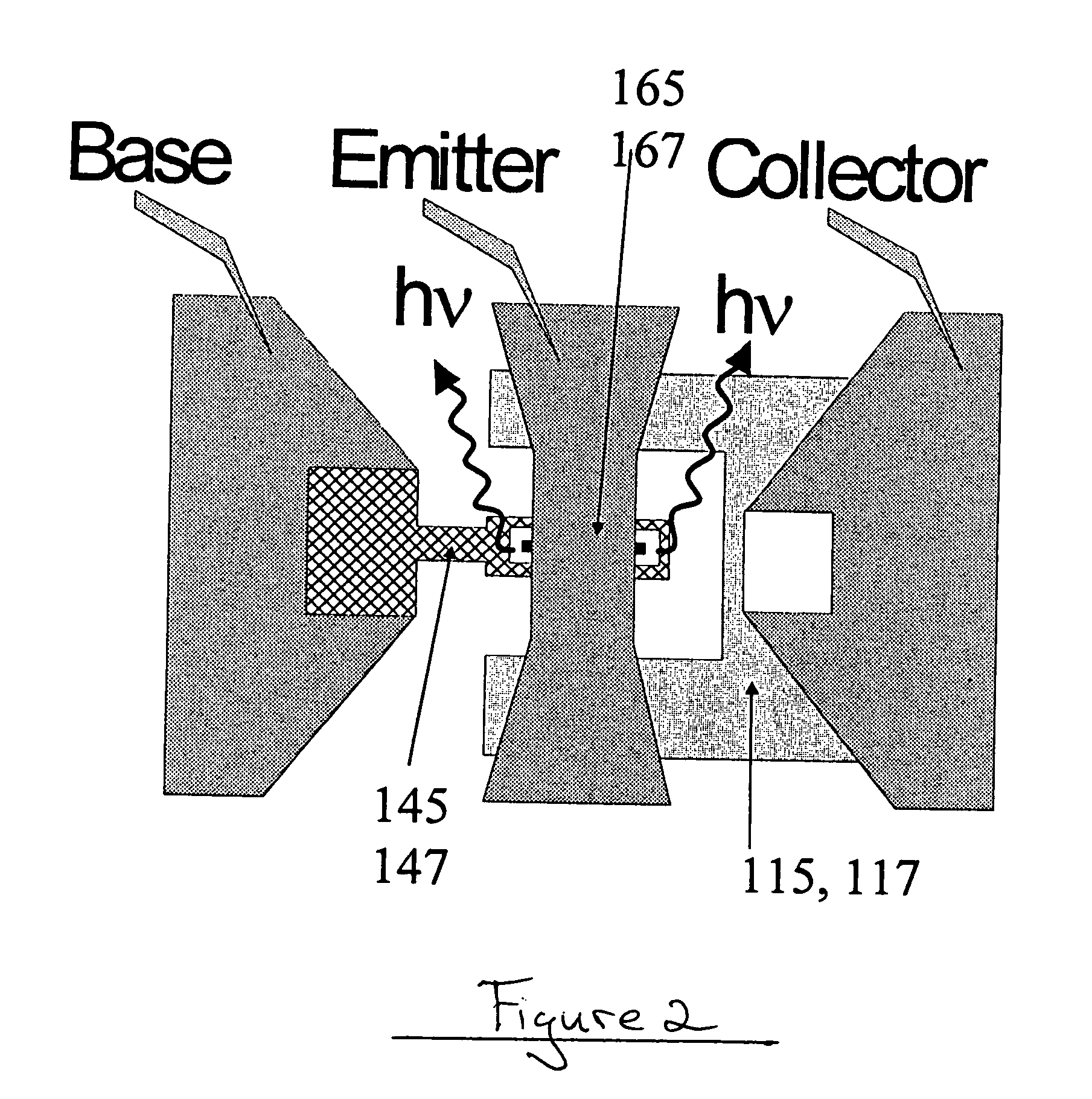
[0045]FIG. 1 illustrates a device in accordance with an embodiment of the invention and which can be used in practicing an embodiment of the method of the invention. A substrate 105 is provided, and the following layers are disposed thereon: subcollector 110, collector 130, base 140, emitter 150, and cap layer 160. Also shown are collector metallization (or electrode) 115, base metallization 145, and emitter metallization 165. Collector lead 117, base lead 147, and emitter lead 167 are also shown. In a form of this embodiment, the layers are grown by MOCVD, and the collector layer 130 comprises 3000 Angstrom thick n-type GaAs, n=2×1016 cm−3, the base layer 140 comprises 600 Angstrom thick p+ carbon-doped compositionally graded InGaAs (1.4% In), p=4.5×1019 cm−3, the emitter layer 150 comprises 800 Angstrom thick n-type InGaP, n=5×1017 cm−3, and the cap layer comprises 1000 Angstrom thick n+ InGaAs, n=3×1019 cm−3.

[0046]This embodiment employs a fabrication process sequence which inclu...


PUM


Abstract

A method for increasing the speed of a bipolar transistor, includes the following steps: providing a bipolar transistor having emitter, base, and collector regions; providing electrodes for coupling electrical signals with the emitter, base, and collector regions; and adapting the base region to enhance stimulated emission to the detriment of spontaneous emission, so as to reduce carrier recombination lifetime in the base region.

Description

RELATED APPLICATION[0001]This is a continuation-in-part of U.S. patent application Ser. No. 10 / 646,457, filed Aug. 22, 2003, now abandoned and said application is incorporated herein by reference. The subject matter of the present application is related to subject matter of copending U.S. patent application Ser. No. 10 / 861,103 (UI-TF-04036), filed of even date herewith, and assigned to the same assignee as the present application.FIELD OF THE INVENTION[0002]This invention relates to high speed semiconductor devices and methods, and also to semiconductor devices and methods for producing controlled light emission, and which are also simultaneously capable of electrical signal amplification.BACKGROUND OF THE INVENTION[0003]A part of the background hereof lies in the development of light emitters based on direct bandgap semiconductors such as III-V semiconductors. Such devices, including light emitting diodes and laser diodes, are in widespread commercial use.[0004]Another part of the ...

Claims


Application Information

Patent Timeline
Patent Type & Authority Patents(United States)
IPC IPC(8): H01L21/8249H01L21/00H01L29/739H01L31/0328H01L31/109H01L33/00H01L33/08
CPCH01L33/0016H01L33/08H01L29/0821H01L29/1004H01L29/155H01L29/205H01L29/66242H01L29/7371
Inventor FENG, MILTONHOLONYAK, JR., NICK
Owner THE BOARD OF TRUSTEES OF THE UNIV OF ILLINOIS
Why Eureka
Try Eureka