Front-end circuit of the wireless transceiver

a wireless transceiver and front-end circuit technology, applied in transmission, multiple-port network, electrical apparatus, etc., can solve the problems of reducing output power, increasing noise figure, and reducing output power, so as to reduce noise figure and increase output power

Active Publication Date: 2011-09-20
AIROHA TECHNOLOGY CORPORATION
View PDF8 Cites 11 Cited by
  • Summary
  • Abstract
  • Description
  • Claims
  • Application Information

AI Technical Summary

Benefits of technology

[0007]Therefore, a front-end circuit of the wireless transceiver is disclosed to overcome the foregoing problems according to the present invention, especially, it is with fewer pin count of the chip, furthermore, the noise figure can be reduced with respect to the signal receiving path, or the output power can be increased with respect to the signal transmitting path.
[0008]An object of the present invention is to provide a front-end circuit of the wireless transceiver, wherein the noise figure can be reduced accordingly since the signal is passed through the receiving path that is between the receiver and the antenna unit without the switch.
[0009]Another object of the present invention is to provide a front-end circuit of the wireless transceiver, wherein the output power can be increased accordingly since the signal is passed through the transmitting path that is between the transmitter and the antenna unit without the switch.
[0010]Another object of the present invention is to provide a front-end circuit of the wireless transceiver, wherein the switch, the second impedance matching circuit, the transmitter, and the receiver are integrated within a single chip, thereby, the pin count of the chip can be reduced, as well as, the second impedance matching circuit can be selectively provided for demand.
[0011]Another object of the present invention is to provide a front-end circuit of the wireless transceiver, wherein the second impedance matching circuit is provided within the transmitting block for reducing the noise figure of the receiving path, thereby, the impedance matching between the antenna unit and the transmitting path can be achieved when the front-end circuit is operating on transmitting mode. And the impedance matching between the antenna unit and the receiving path can also be achieved when the front-end circuit is operating on receiving mode.
[0012]Another object of the present invention is to provide a front-end circuit of the wireless transceiver, wherein the second impedance matching circuit is provided within the receiver, therefore, the output power can be increased with respect to the transmitting path, such that the impedance matching between the antenna unit and the transmitting path can be achieved when the front-end circuit is operating on transmitting mode. And the impedance matching between the antenna unit and the receiving path can be achieved when the front-end circuit is operating on receiving mode.

Problems solved by technology

However, signal pass through the switches 13 and 23 would causes the signal loss, such that the noise figure will be increased on the process of receiving signal, as well as, the output power will be degraded on the process of transmitting signal, thereby, the front-end circuits 10 and 20 cannot be applied for the wireless transceiver that demands low noise figure or high output power.

Method used


Image

  • Front-end circuit of the wireless transceiver
  • Front-end circuit of the wireless transceiver
  • Front-end circuit of the wireless transceiver

Examples


Embodiment Construction

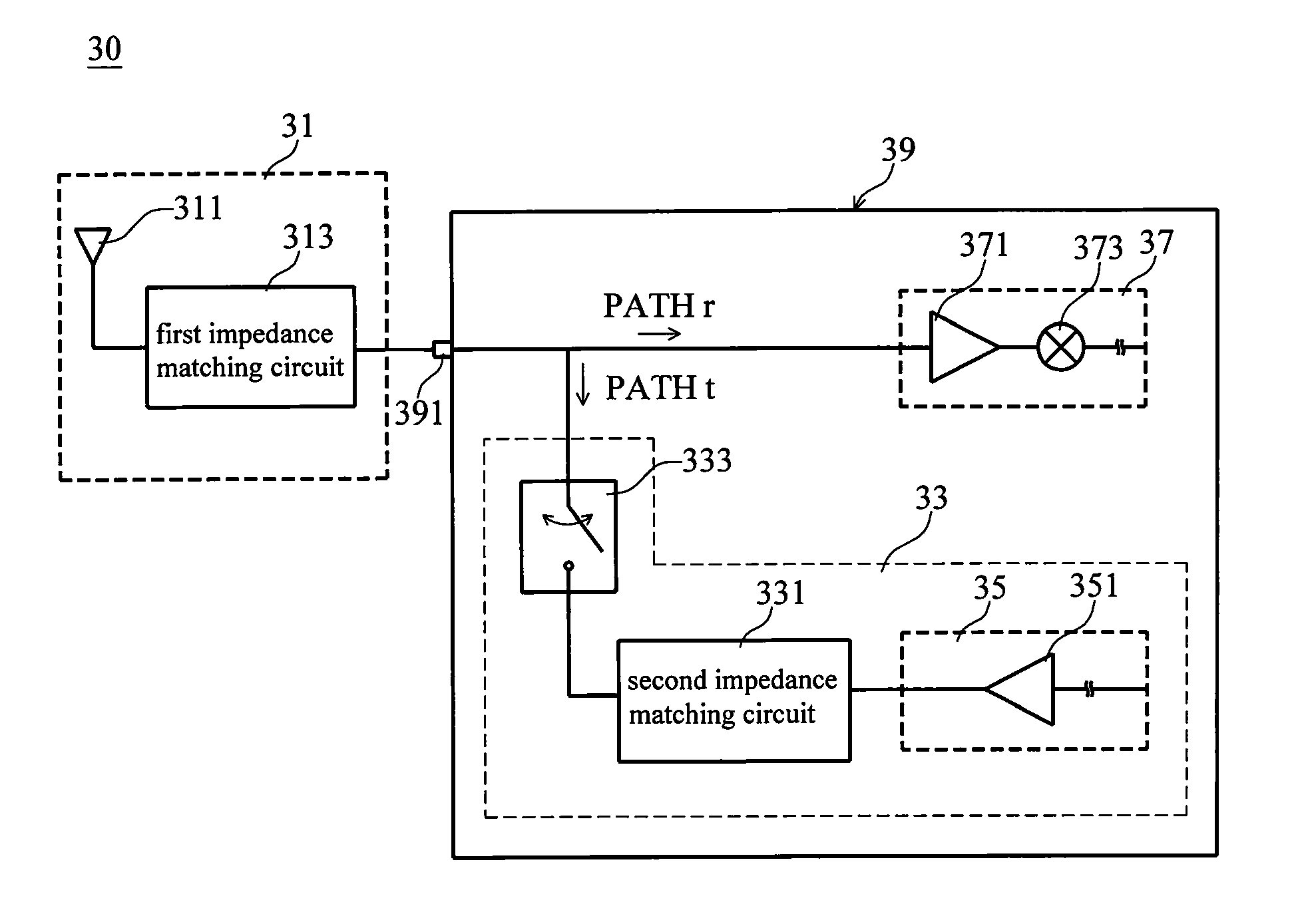
[0025]Referring to FIG. 3, a block diagram showing a front-end circuit of the wireless transceiver in accordance with an embodiment of the present invention is disclosed. The wireless transceiver comprises a front-end circuit 30 and a back end circuit, wherein the front-end circuit 30 comprises an antenna unit 31, a receiver 37, and a transmitting block 33, all of which are connected.

[0026]The antenna unit 31 of the front-end circuit 30 comprises an antenna 311 and a first impedance matching circuit 313, as well as, the antenna unit 31 is used as a transmission interface for the receiving or transmitting wireless signal. The receiver 37 and the transmitting block 33 are integrated within a single chip 39, having the pin 391 for connecting to the first impedance matching circuit 313 of the antenna unit 31. While the antenna unit 31 is receiving the wireless signal, the signal will be sent to the chip 39 through the pin 391, as well as, while the antenna unit 31 is transmitting the wi...


PUM


Abstract

A front-end circuit of the wireless transceiver is disclosed to reduce the number of the pin count of the chip, and achieve the impedance matching. The circuit comprises an antenna unit, a receiver, and a transmitting block, all of which are connected together, wherein there is no switch provided between the receiver and the antenna unit, such that the loss of switch can be avoided for reducing the noise figure and improve the sensitivity of the receiving path accordingly.

Description

FIELD OF THE INVENTION[0001]The present invention relates to a front-end circuit of the wireless transceiver, and more particularly to a front-end circuit of the wireless transceiver that can be used to reduce the number of the pin count of the chip and achieve the impedance matching.BACKGROUND OF THE INVENTION[0002]Referring to FIG. 1, a block diagram of wireless transceiver with respect to the prior art is showed. The transceiver comprises a front-end circuit 10 and a back end circuit, wherein the front-end circuit 10 is used for transmitting and receiving wireless signal, comprising an antenna unit 11, a switch 13, a receiver 171 and a transmitter 173, wherein the receiver 171 and the transmitter 173 are integrated into a single chip 17.[0003]The switch 13 is used for controlling the wireless transceiver to transmit or receive signal. While the front-end circuit 10 is receiving the signal, the switch 13 can switch to “a” terminal, thereby, the antenna unit 11 will be connected to...

Claims


Application Information

Patent Timeline
Patent Type & Authority Patents(United States)
IPC IPC(8): H01P1/10H04B1/44
CPCH04B1/18
Inventor LEE, CHIEN-KUANG
Owner AIROHA TECHNOLOGY CORPORATION
Why Eureka
Try Eureka