
Spray method for producing semiconductor nano-particles

a nano-particle and nano-particle technology, applied in the direction of coatings, transportation and packaging, mercury compounds, etc., can solve the problems of nano-particle doping, limited liberty to choose the substrate, and high cost, and achieve the effect of preventing adverse liquid solvent effects

Inactive Publication Date: 2011-10-04
TECHNION RES & DEV FOUND LTD
View PDF14 Cites 1 Cited by
  • Summary
  • Abstract
  • Description
  • Claims
  • Application Information

AI Technical Summary

Benefits of technology

[0008]The method provided by the present invention produces high quality nanoparticles that are characterized by several new and unique features and advantages not exhibited by nanoparticles produced by currently available methods.
[0012]The step of collecting the unsupported semiconductor nanoparticles on a solid support typically produces a highly closed packed array. Alternatively, it can be used for producing a two or three-dimensional array of said nanoparticles. Said solid support may be heated and maintained at a selected temperature to prevent adverse liquid solvent effects.

Problems solved by technology

This method requires ultra high vacuum as well as other complex and expensive equipment.
Furthermore, the liberty to choose the substrate is limited.
The colloidal method enables the reproducible but not continued formation of nanoparticles, with a variety of sizes and shapes, with initial distributions of 10<σ<20% in diameter, and with some control on surface properties, but it does not allow doping of the nanoparticles.
Furthermore, the organic capping has a key role in any self-assembly created by these nanoparticles and prevents a highly packed structure and induces undesirable and hard to control surface properties due to the role of the ligands (namely, the organic molecules attached to the nanoparticle surface as a monolayer through covalent, dative or ionic bonds).

Method used


Image

  • Spray method for producing semiconductor nano-particles
  • Spray method for producing semiconductor nano-particles
  • Spray method for producing semiconductor nano-particles

Examples


example 1

Production of CdS Nanocrystals by Pneumatic Assisted Thermospray

[0073]Cadmium sulfide nanocrystals were intensively investigated in the past few years and thus serve as a good sample for demonstrating the method of the present invention.

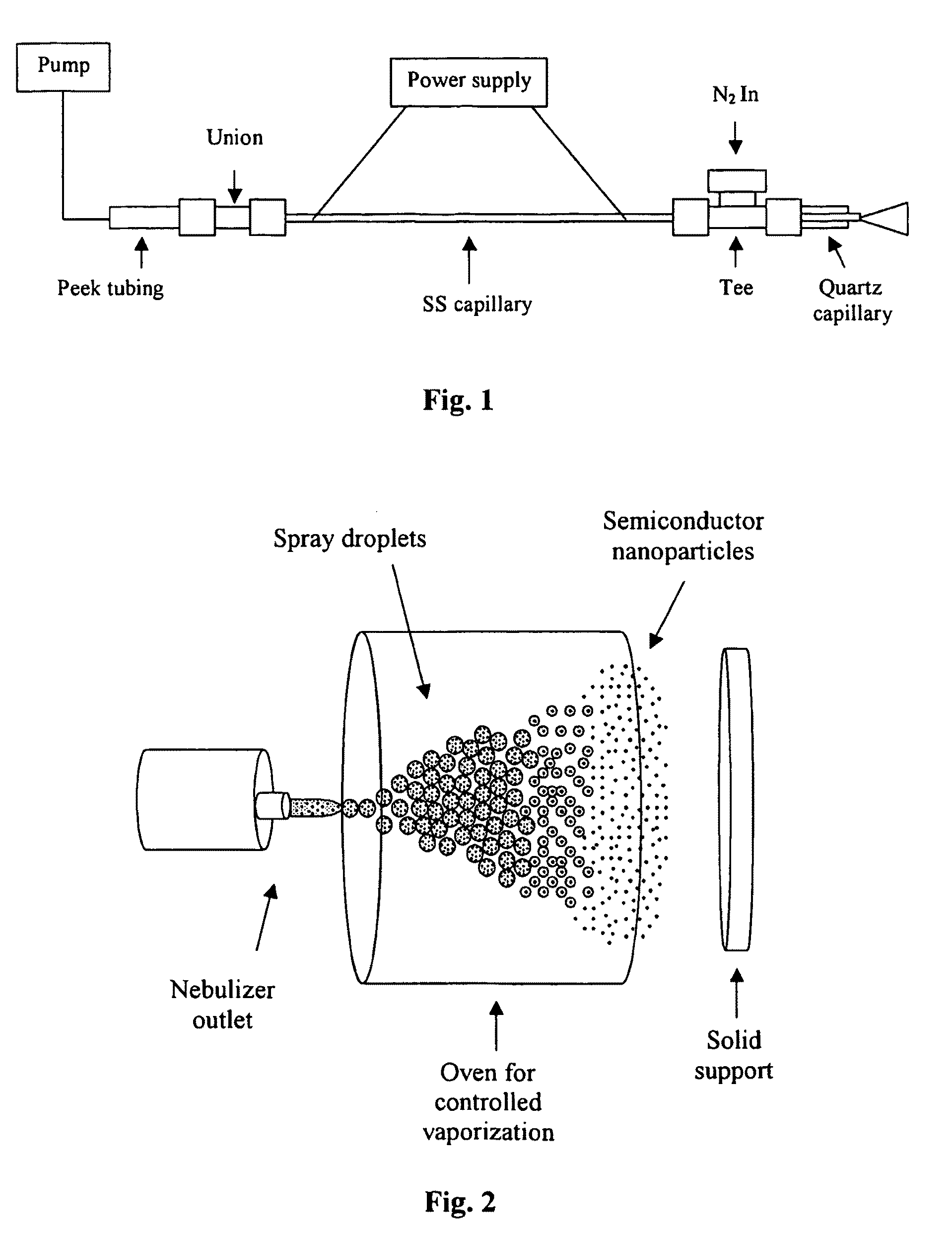
[0074]Cadmium sulfide powder (commercially available from Aldrich) was dissolved in HPLC grade methanol. Spray of droplets of the solution of cadmium sulfide was generated using pneumatic assisted thermospray. The thermospray apparatus employed a stainless steel capillary (0.005″ ID, 0.020″ OD, 20 cm long), with liquid pumped through it by an HPLC pump (model PU-1585, JASCO, Japan) and through a polyetheretherketone (PEEK) tubing (0.0025″ ID, 1 / 16″ OD). The PEEK tubing was connected to the stainless steel capillary by a PEEK union. A heating power supply (Manson NP-9613) was connected to two points on the capillary, by specially designed clamps. The positive point was located near the inlet side and the negative point was located about 8 cm further d...

example 2

Production of CdS Nanocrystals by Pneumatic Assisted Electrospray

[0078]Cadmium sulfide powder (commercially available from Aldrich) is dissolved in HPLC grade methanol. Spray of droplets of the solution of cadmium sulfide is generated using electrospray. The electrospray apparatus employs a stainless steal (SS) capillary (0.005″ ID, 0.020″ OD, 10 cm long, Upchurch), with liquid pumped through it by an HPLC pump (model PU-1585, JASCO) and through a PEEK tubing (0.0025″ ID, 1 / 16″ OD). The PEEK tubing is connected to the SS capillary by a PEEK union. A high-voltage power supply (Stanford, model PS 350) is connected to the outlet of the capillary. The capillary is then entered into a PEEK tee-shaped structure in order to supply a nitrogen gas flow for pneumatic assistance. The gas flows out of the tee through a quartz tube surrounding the capillary. A Kanthal wire is looped on the quartz tube and serves as a heating source. The spray is collected on the desired substrate, which serves a...


PUM

PropertyMeasurementUnit
diameteraaaaaaaaaa
diameteraaaaaaaaaa
diameteraaaaaaaaaa

Abstract

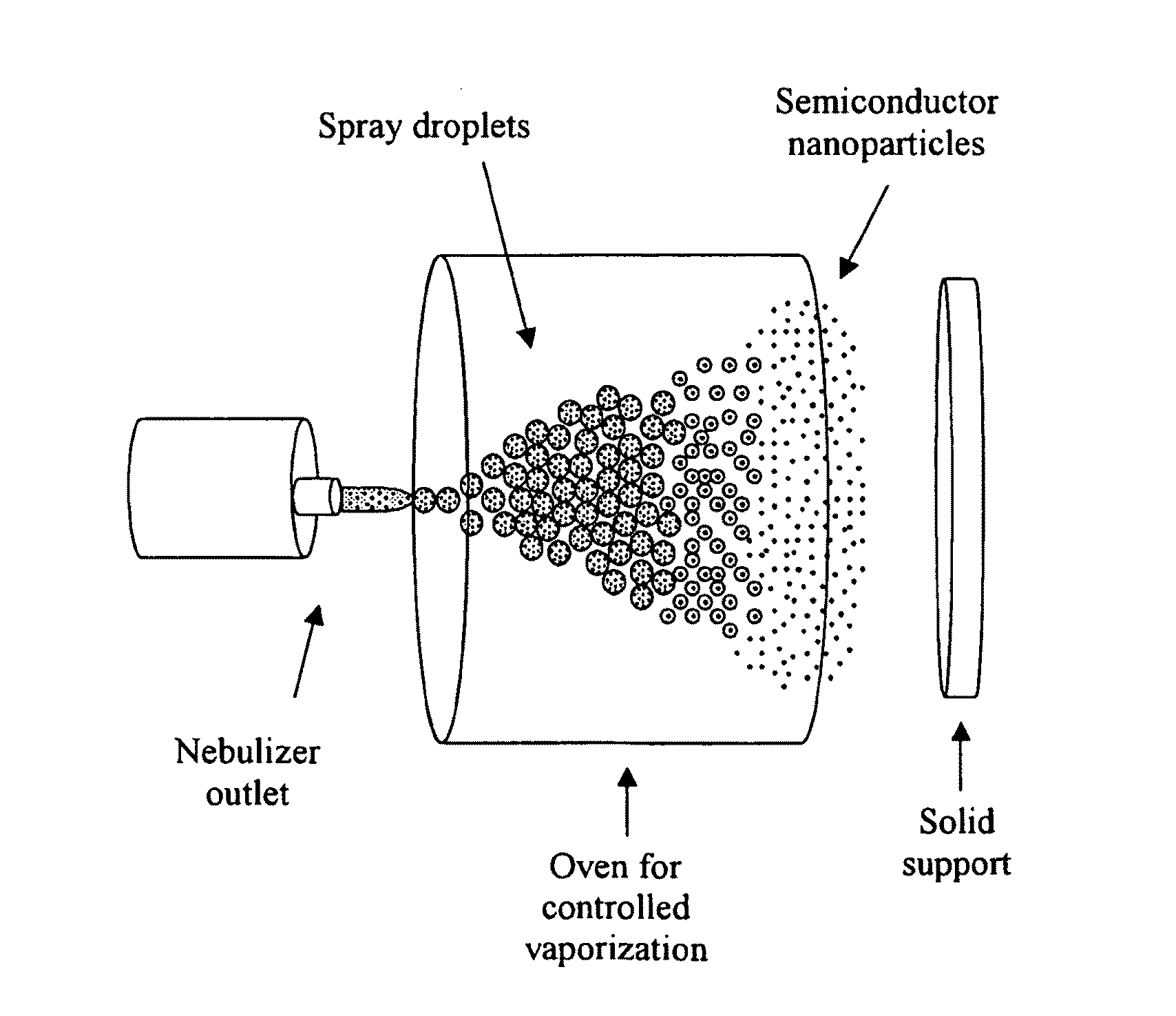
A method is provided for producing semiconductor nanoparticles comprising: (i) dissolving a semiconductor compound or mixture of semiconductor compounds in a solution; (ii) generating spray droplets of the resulting solution of semiconductor compound(s); (iii) vaporizing the solvent of said spray droplets, consequently producing a stream of unsupported semiconductor nanoparticles; and (iv) collecting said unsupported semiconductor nanoparticles on a support.

Description

FIELD OF THE INVENTION[0001]The present invention relates to a method for producing semiconductor nanoparticles.BACKGROUND OF THE INVENTION[0002]In the last two decades significant attention has been devoted to the physics of low dimensional semiconductor structures. Among those, semiconductor nanoparticles are of particular interest, due to the pronounced influence of the three-dimensional size confinement on their electronic and optical properties. Extensive effort has been devoted for the production of high quality semiconductor nanoparticles, motivated by their potential use in new and emerging technologies.[0003]Currently, there are two main methods for the fabrication of semiconductor nanoparticles, namely epitaxial growth and colloidal chemistry techniques. Epitaxial growth of nanoparticles on top of a substrate with a different lattice constant leads to strain induced three-dimensional islands, known as Stranski Krastanow (SK) quantum dots.[0004]The SK method produces relati...

Claims


Application Information

Patent Timeline
Patent Type & Authority Patents(United States)
IPC IPC(8): H01L21/00B22F1/054B22F1/102B22F1/16
CPCB22F1/0018B22F1/02B22F9/04B82Y30/00C01B19/007C01G9/08C01G11/02C01G13/00C01G15/00C23C4/121C01P2004/04C01P2004/51C01P2004/64C01P2006/40Y10S977/84C23C4/123B22F1/054B22F1/16B22F1/102
Inventor AMIRAV, LILACLIFSHITZ, EFRAT
Owner TECHNION RES & DEV FOUND LTD
Learn More