Semiconductor device with a gate having a bulbous area and a flattened area underneath the bulbous area and method for manufacturing the same

a technology of semiconductor devices and bulbous areas, applied in semiconductor devices, electrical devices, transistors, etc., can solve the problems of increasing the difficulty of achieving a desired threshold voltage using conventional planar channel structures, affecting the performance of semiconductor devices, and requiring alternate solutions, so as to prevent or at least minimize the degradation of refresh characteristics

Active Publication Date: 2011-10-04
SK HYNIX INC
View PDF8 Cites 0 Cited by
  • Summary
  • Abstract
  • Description
  • Claims
  • Application Information

AI Technical Summary

Benefits of technology

[0009]Embodiments of the present invention are directed to a semiconductor device that can prevent or at least minimize the degradation of refresh characteristics from occurring and a method for manufacturing the same.
[0010]Also, embodiments of the present invention are directed to a semiconductor device that can reduce GIDL (gate-induced drain leakage) and a method for manufacturing the same.

Problems solved by technology

As high integration of a semiconductor device proceeds, it is becoming more and more difficult to achieve a desired threshold voltage using conventional planar channel structures.
Thus, limitations arise and alternate solutions must be present that can overcome these problems brought about by the high integration.
Unfortunately, semiconductor devices having the saddle fin-shaped channel can suffer a threshold voltage problem.
However, if this is the case, then electric fields in junction areas are intensified, and the junction leakage increases.
As a result the refresh characteristics are likely to degrade.
Meanwhile, in the case where the existing dry oxidation scheme is employed instead of the radical gate oxidation scheme, degradations in terms of sub-threshold slope and DIBL (drain-induced barrier lowering) arise, whereby off-leakage increases and refresh characteristics are also likely to deteriorate.

Method used


Image

  • Semiconductor device with a gate having a bulbous area and a flattened area underneath the bulbous area and method for manufacturing the same
  • Semiconductor device with a gate having a bulbous area and a flattened area underneath the bulbous area and method for manufacturing the same
  • Semiconductor device with a gate having a bulbous area and a flattened area underneath the bulbous area and method for manufacturing the same

Examples


Embodiment Construction

[0038]Hereafter, specific embodiments of the present invention will be described in detail with reference to the accompanying drawings.

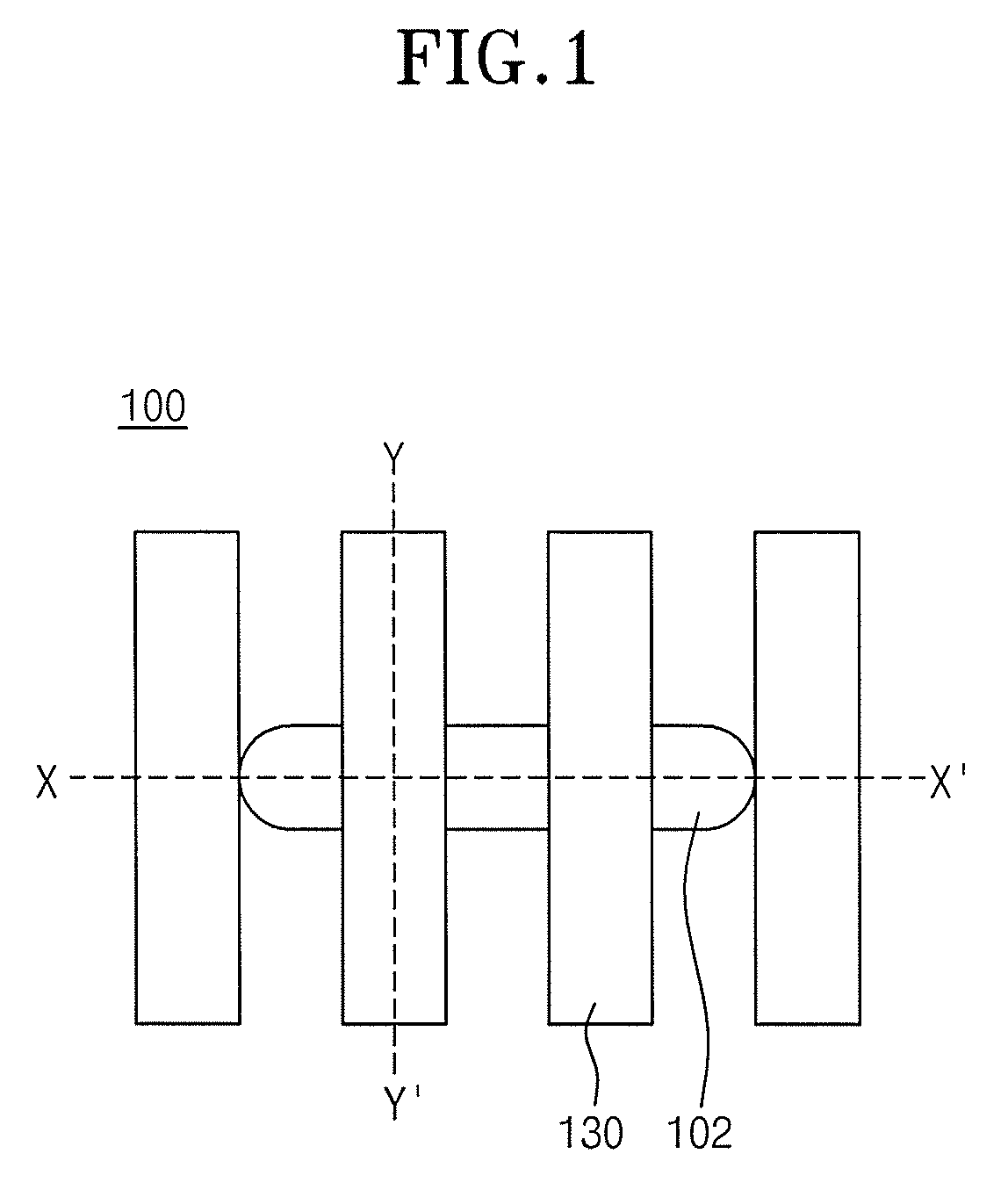
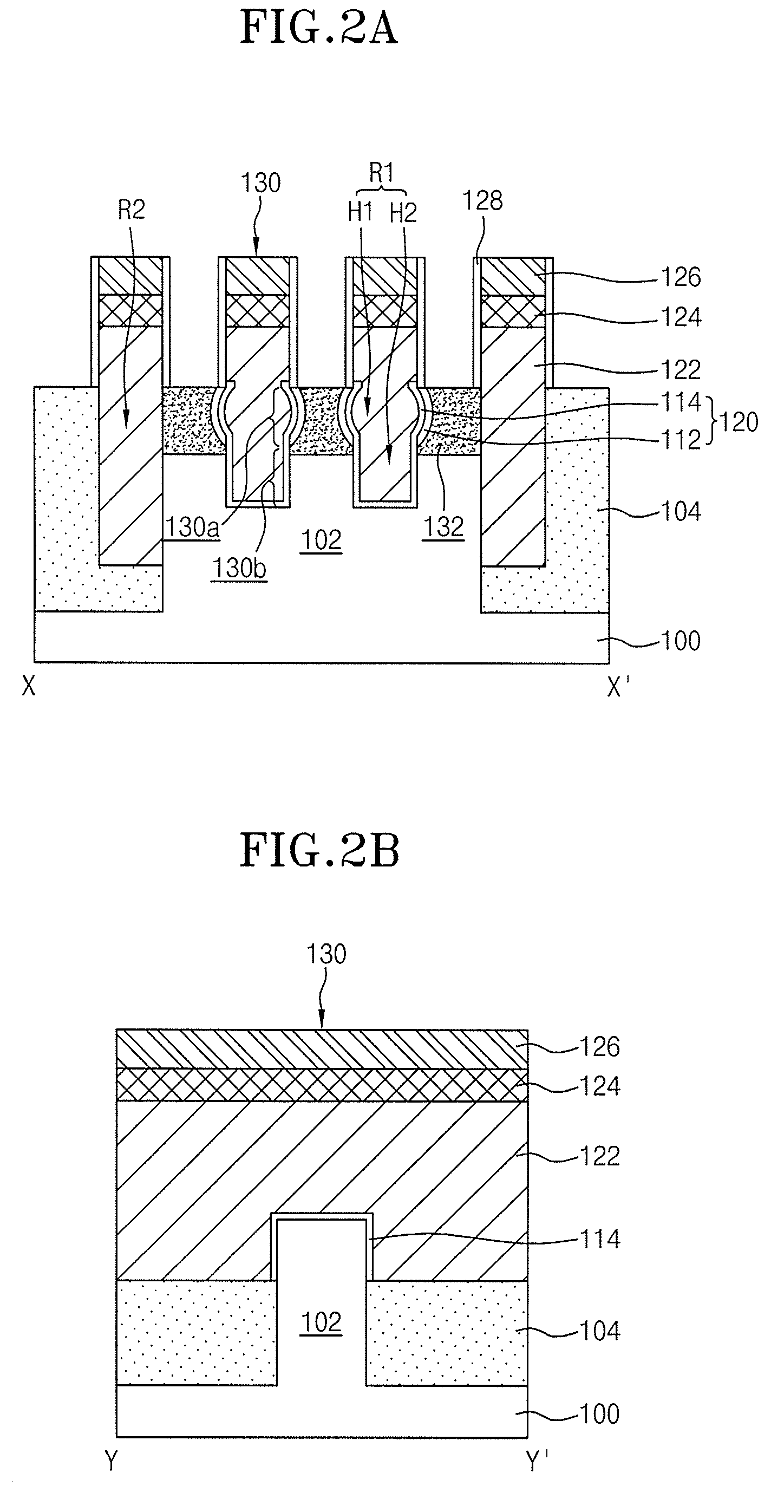
[0039]FIG. 1 is a plan view illustrating a semiconductor device in accordance with an embodiment of the present invention, and FIGS. 2A and 2B are sectional views taken along the lines X-X′ and Y-Y′, respectively, of FIG. 1.

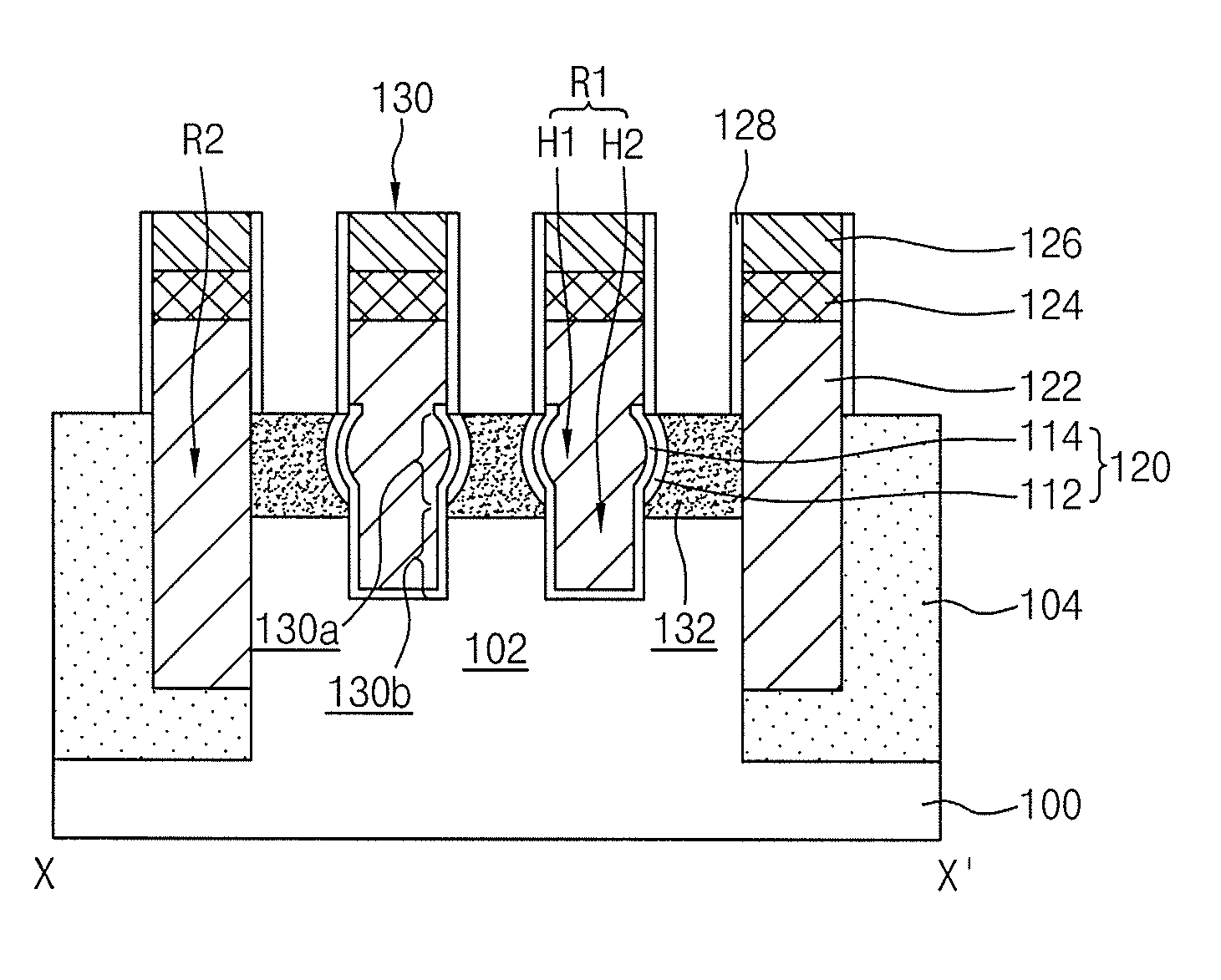
[0040]Referring to these drawings, an isolation layer 104 is formed in a semiconductor substrate 100 to delimit an active region 102. First recess parts R1 are defined in the gate forming areas of the active region 102 to a first depth. Second recess parts R2 are defined in portions of the isolation layer 104, which extend from the gate forming areas, to a second depth greater than the first depth to expose the front and rear surfaces of the gate forming areas recessed to the first depth, that is, to obtain a saddle fin-shaped channel. Each first recess part R1 is composed of a first groove H1 which is defined in the surface of th...


PUM


Abstract

A semiconductor device with a gate having a bulbous area and a flattened area underneath the bulbous are is presented. The semiconductor device includes a semiconductor substrate, an isolation layer, a gate insulation layer, and gates. The semiconductor substrate has recess parts that have first grooves which have bulbous-shaped profiles and second vertically flattened profile grooves which extend downward from the first grooves. The gates are formed in the recess parts in which the gate insulation layer is double layered in the bulbous profile areas and is single layered in the flattened profile areas.

Description

CROSS-REFERENCE TO RELATED APPLICATIONS[0001]The present application claims priority to Korean patent application number 10-2009-0015115 filed on Feb. 24, 2009, which is incorporated herein by reference in its entirety.BACKGROUND OF THE INVENTION[0002]The present invention relates to a semiconductor device and a method for manufacturing the same, and more particularly, to a semiconductor device that can realize a reduction in GIDL (gate-induced drain leakage) and a method for manufacturing the same.[0003]As high integration of a semiconductor device proceeds, it is becoming more and more difficult to achieve a desired threshold voltage using conventional planar channel structures. Thus, limitations arise and alternate solutions must be present that can overcome these problems brought about by the high integration. Under these circumstances, research has actively been conducted in order to develop semiconductor devices which have three-dimensional channel structures capable of securi...

Claims


Application Information

Patent Timeline
Patent Type & Authority Patents(United States)
IPC IPC(8): H01L29/76
CPCH01L29/66621H01L29/4236H01L29/4232H01L29/66348
Inventor CHUN, SUNG GIL
Owner SK HYNIX INC
Why Eureka
Try Eureka