In-line voltage contrast detection of PFET silicide encroachment

a technology of in-line voltage contrast and silicide encroachment, which is applied in the direction of individual semiconductor device testing, semiconductor/solid-state device testing/measurement, instruments, etc., can solve the problems of consuming a large area of probe pads, affecting cmos technology, and killing associated devices

Inactive Publication Date: 2011-10-18
INT BUSINESS MASCH CORP
View PDF5 Cites 86 Cited by
  • Summary
  • Abstract
  • Description
  • Claims
  • Application Information

AI Technical Summary

Problems solved by technology

This silicide is susceptible to migration causing shorts between the drain, body, source and gate which effectively kill the associated device.
This defect mechanism, which may be referred to as silicide encroachment, is one of the top causes of yield loss affecting the CMOS technology.
However, since leakages just one thousand times greater than the leakage of a good CMOS device may be sufficient to kill a device, only small numbers of devices may be tied together and tested simultaneously.
The area required for probe pads consumes much more area than the CMOS structures themselves.
A second disadvantage of using probe-able test structures is that time intensive failure analysis and scrapping of the entire wafer are required to isolate the actual encroachment defect.
A third disadvantage is that the structures are only tested at metal 1 or later, which is long after the encroachment defects may have formed.
However, detection of encroachment defects affecting PFET devices has proven to be more challenging, due to insufficient contrast when the VC inspection is applied.

Method used


Image

  • In-line voltage contrast detection of PFET silicide encroachment
  • In-line voltage contrast detection of PFET silicide encroachment
  • In-line voltage contrast detection of PFET silicide encroachment

Examples


Embodiment Construction

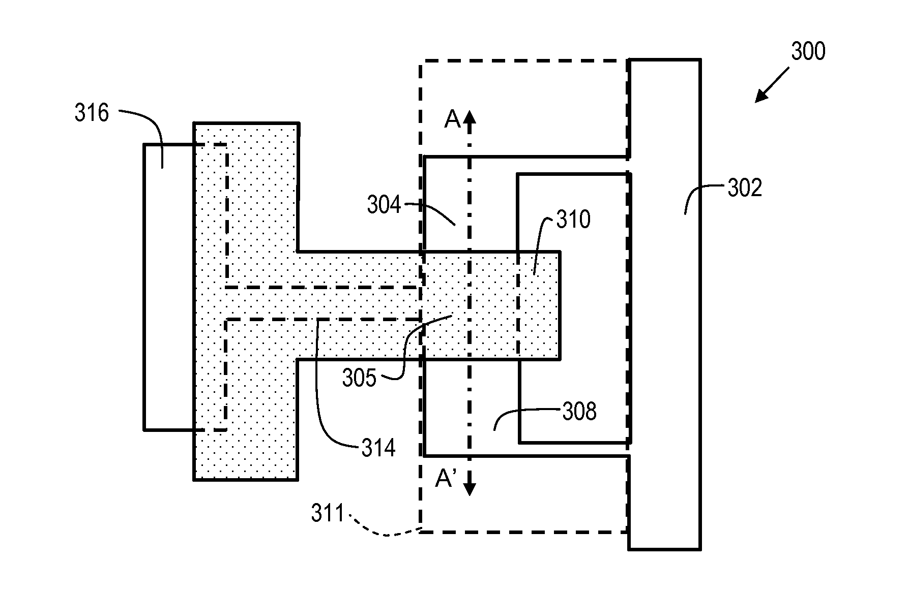
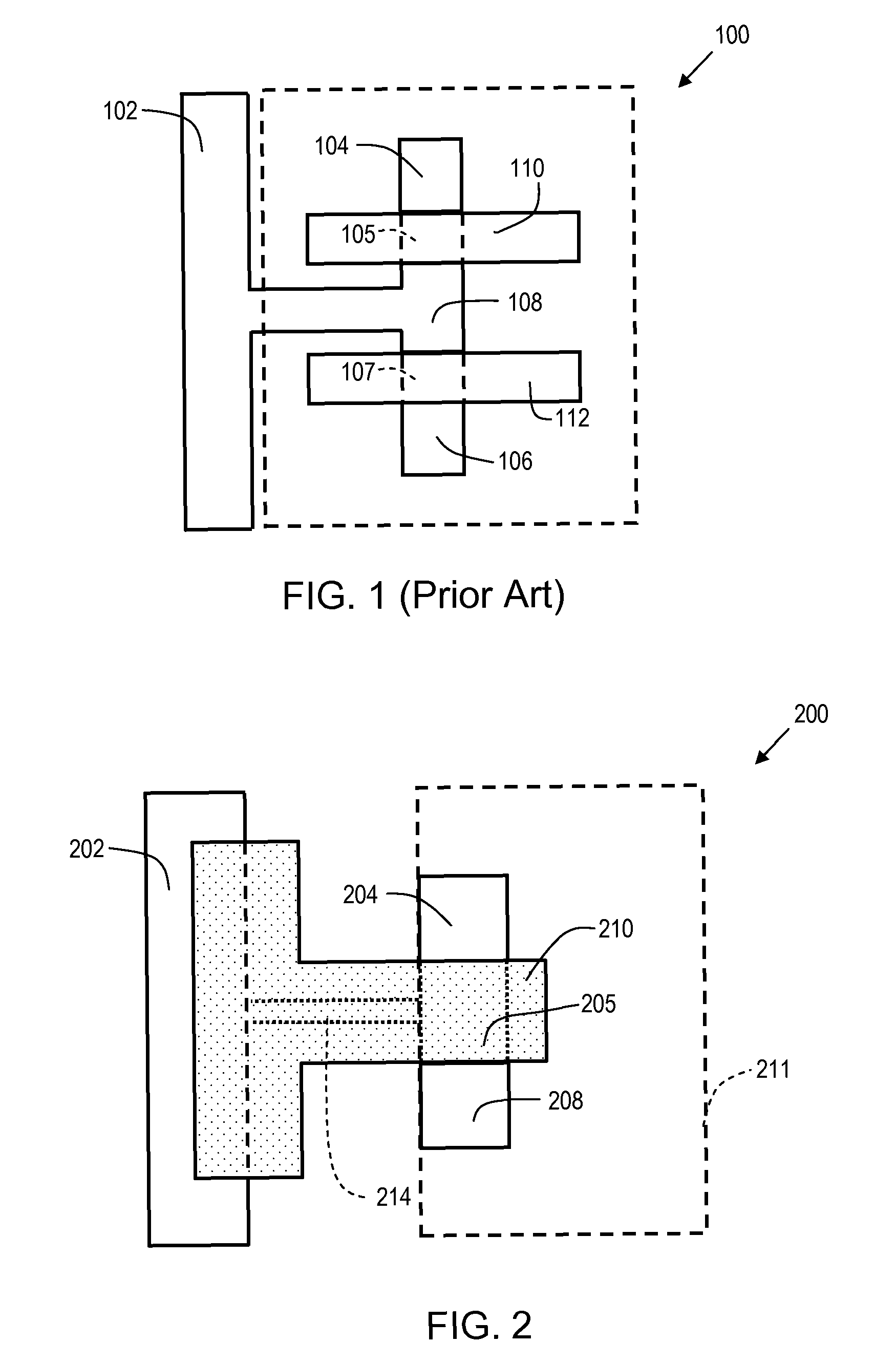
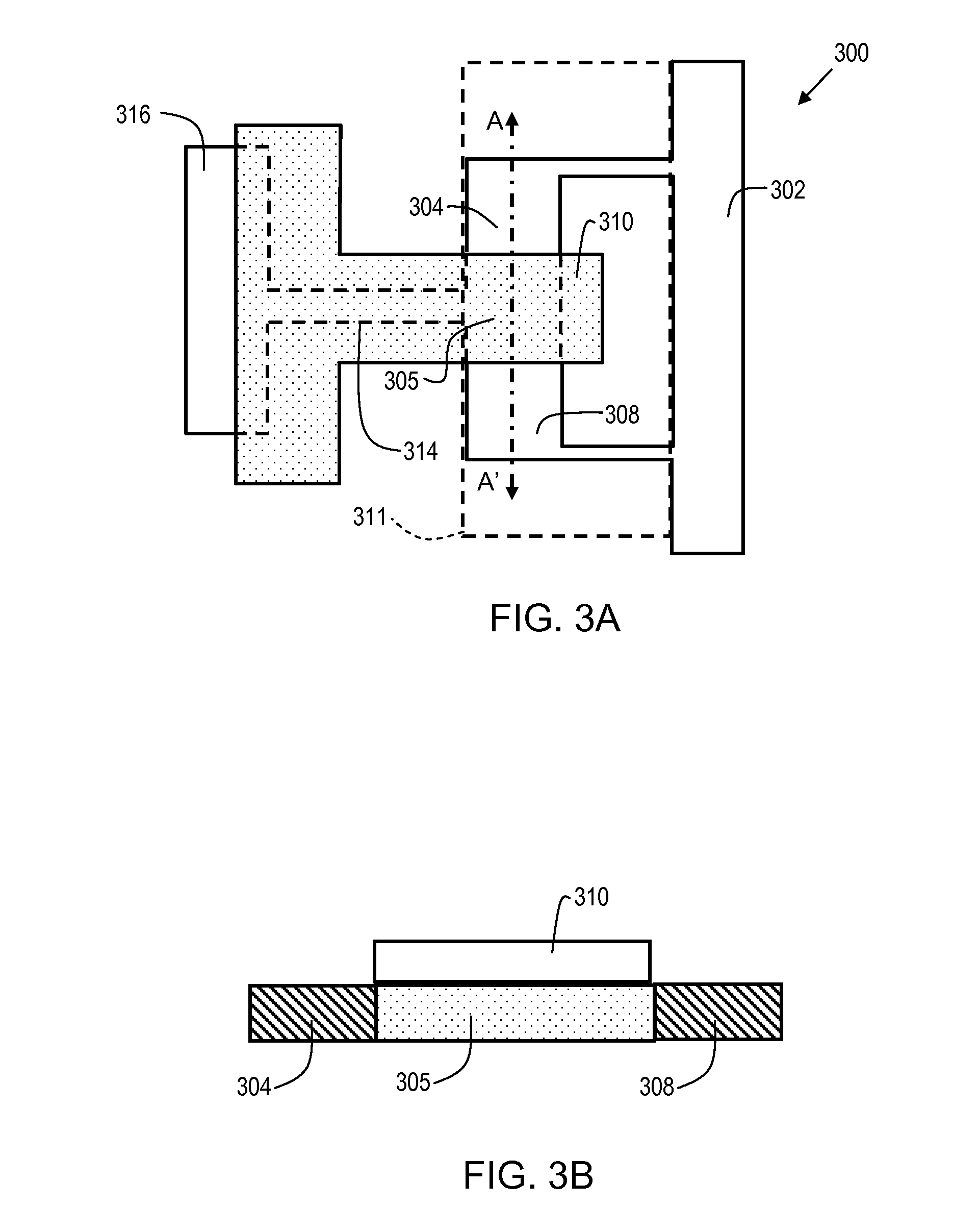
[0023]In order to provide some context for the description of embodiments of the present invention, the prior art structure of FIG. 1 will be briefly described below. FIG. 1 shows a test structure 100 which is used for NFET evaluation. The test structure 100 is comprised of N+ source regions 104 and 106, and gate stacks 110 and 112. N+ drain region 108 is disposed between gate stacks 110 and 112. Therefore, test structure 100 is essentially comprised of two NFET transistors in series, with the common drain 108 grounded via connection to ground bus 102. Therefore, the junction between N+ source region 104, and P+ region 105 (which is under gate stack 110) is an NP junction. Similarly, the junction between N+ source region 106 and P+ region 107 (which is under gate stack 112) is an NP junction.

[0024]When a SEM electron beam scans the surface of test structure 100, the primary electrons emitted by the SEM cause more secondary electrons to be ejected from the N+ source regions 104 and 1...


PUM


Abstract

A semiconductor test structure includes a PFET transistor, having a source region, a drain region, a gate disposed between the source region and the drain region, a body disposed under the gate, and a body contact. The source region and drain region float, and the body contact is electrically connected to the body of the PFET transistor and to the ground. This grounds the body of the PFET transistor, and the body contact of the test structure is electrically connected to a capacitor that is electrically connected to ground.

Description

FIELD OF THE INVENTION[0001]The present invention relates generally to semiconductor fabrication and, more particularly, to test structures for detecting defects using voltage contrast inspection.BACKGROUND OF THE INVENTION[0002]Semiconductor devices or “ICs” (integrated circuits) have evolved from a handful of interconnected devices fabricated on a single chip of silicon to millions of devices. Current ICs provide performance and complexity far beyond what was originally imagined. In order to achieve improvements in complexity and circuit density (i.e., the number of devices capable of being packed onto a given chip area), the size of the smallest device feature, also known as the device “geometry,” has become smaller with each generation of ICs. Semiconductor devices are now being fabricated with features less than 50 nanometers across.[0003]Today's CMOS technologies utilize silicide to reduce the resistivity of the active and poly-silicon gate regions and allow ohmic contact with...

Claims


Application Information

Patent Timeline
Patent Type & Authority Patents(United States)
IPC IPC(8): H01L23/58
CPCH01L22/34
Inventor PATTERSON, OLIVER D.AHSAN, ISHTIAQ
Owner INT BUSINESS MASCH CORP
Why Eureka
Try Eureka