Bottom source LDMOSFET structure and method

a metal oxide semiconductor and bottom source technology, applied in the direction of semiconductor devices, semiconductor/solid-state device details, electrical apparatus, etc., can solve the problems of device limitation, device inability to meet the requirements of the device, and the general fabrication cost of the trenched fet device, so as to reduce the cell pitch and reduce the manufacturing cost

Active Publication Date: 2008-01-31
ALPHA & OMEGA SEMICON LTD
View PDF4 Cites 83 Cited by
  • Summary
  • Abstract
  • Description
  • Claims
  • Application Information

AI Technical Summary

Benefits of technology

[0009]It is therefore an aspect of the present invention to provide a new and improved bottom-source lateral diffusion MOS (BS-LDMOS) semiconductor power device implemented with a combined sinker-channel and buried source-body

Problems solved by technology

Conventional technologies to further reduce the source inductance for semiconductor power devices including the source inductance in FET, MOSFET and JFET devices are challenged by several technical difficulties and limitations.
There are difficulties in such approaches due to the facts that typical vertical semiconductor power devices is arranged to place the drain electrode on the substrate.
However, this device has a limitation due to a large cell pitch caused by the lateral spacing required by the top drain contact.
In addition to the limitation of large cell pitch, the trenched FET device in general has a fabrication cost issue due to the fact that the trenched FET requires technologies that may not be available in all foundries and t

Method used


Image

  • Bottom source LDMOSFET structure and method
  • Bottom source LDMOSFET structure and method
  • Bottom source LDMOSFET structure and method

Examples


Embodiment Construction

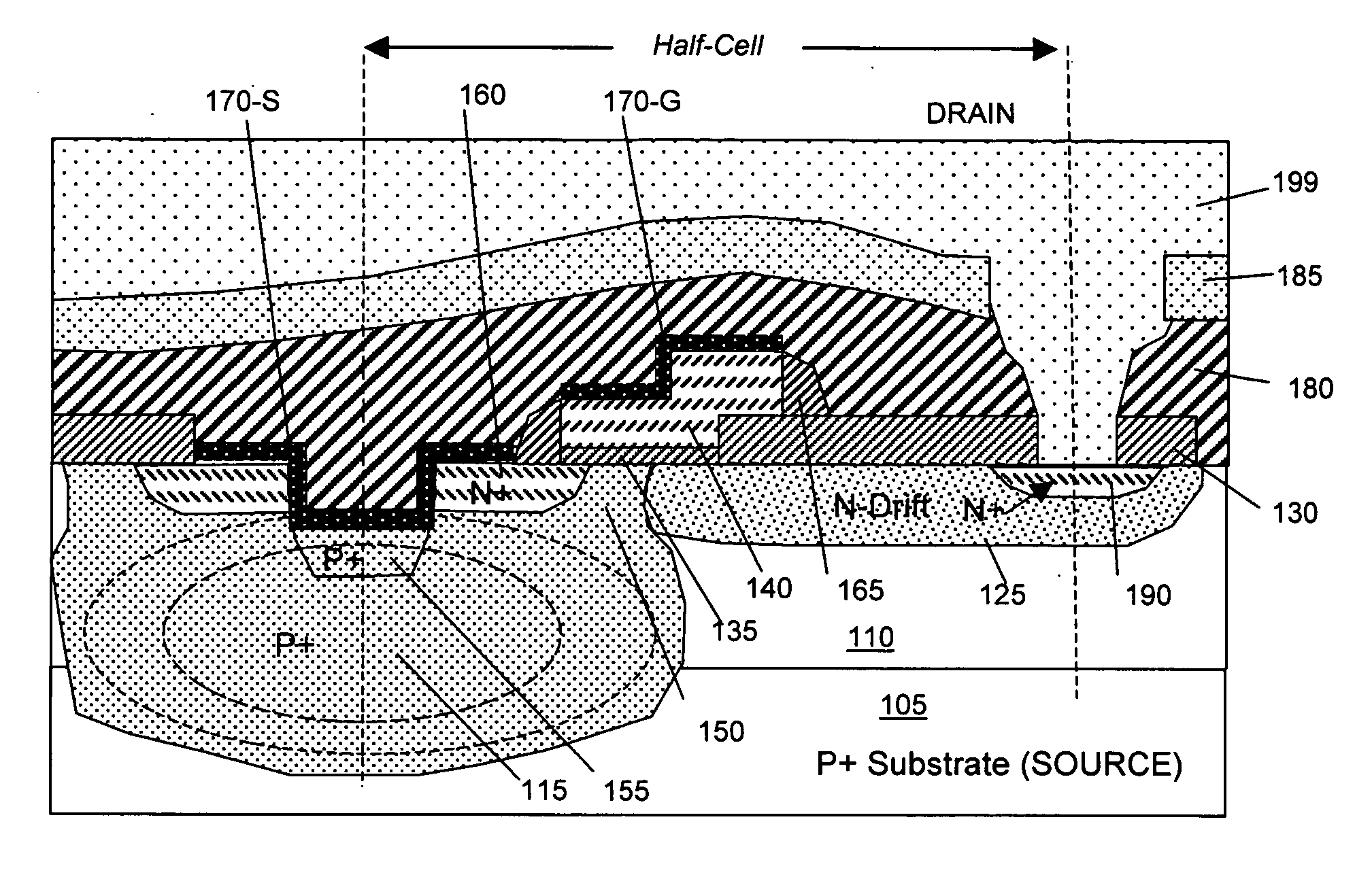
[0027]Referring to FIG. 2 for a cross sectional view of a bottom source (BS) lateral diffusion MOS device of this invention. The BSLDMOS device is supported on a P+ substrate 105 functioning as a bottom source electrode. A layer of P− epitaxial layer 110 is supported on top of the substrate 105. A deep sinker region 115 doped with P+ dopant ions below an active cell area in the device is formed in the epitaxial layer at a depth and extended laterally to a bottom of a drain drift region 125 to compensate some of the N− dopant in the accumulation of the transistor for tailoring a dopant profile of N-drift region 125 to minimize the gate-drain capacitance while maintaining a low drain to source resistance Rdson._The deep sinker region 115 further extends vertically both downward to the bottom P+ substrate 105, and upward to a body region 150 that forms a channel at a top surface under a gate oxide 135. The sinker regions 115 functions as a combined channel and also as a buried source b...


PUM


Abstract

This invention discloses bottom-source lateral diffusion MOS (BS-LDMOS) device. The device has a source region disposed laterally opposite a drain region near a top surface of a semiconductor substrate supporting a gate thereon between the source region and a drain region. The BS-LDMOS device further has a combined sinker-channel region disposed at a depth in the semiconductor substrate entirely below a body region disposed adjacent to the source region near the top surface wherein the combined sinker-channel region functioning as a buried source-body contact for electrically connecting the body region and the source region to a bottom of the substrate functioning as a source electrode. A drift region is disposed near the top surface under the gate and at a distance away from the source region and extending to and encompassing the drain region. The combined sinker-channel region extending below the drift region and the combined sinker-channel region that has a dopant-conductivity opposite to and compensating the drift region for reducing the source-drain capacitance.

Description

BACKGROUND OF THE INVENTION[0001]1. Field of the Invention[0002]The invention relates generally to the semiconductor power devices. More particularly, this invention relates to a bottom-source lateral diffusion metal oxide semiconductor field effect transistor (LDMOSFET) structure and manufacturing methods.[0003]2. Description of the Prior Art[0004]Conventional technologies to further reduce the source inductance for semiconductor power devices including the source inductance in FET, MOSFET and JFET devices are challenged by several technical difficulties and limitations. There are ever increasing demand to reduce the source inductance in the semiconductor power devices because more and more power devices are required to apply in the applications that demand high efficiency, high gain, and high frequency semiconductor power devices. The source inductance reduction can be achieved by eliminating the bond-wires in the package of a semiconductor power device. Many attempts are made to ...

Claims


Application Information

Patent Timeline
IPC IPC(8): H01L23/58H01L21/336
CPCH01L21/26513H01L29/402H01L2924/0002H01L29/4175H01L29/41766H01L29/41775H01L29/42368H01L29/456H01L29/4933H01L29/4941H01L29/66659H01L29/7835H01L2924/13091H01L2924/00H01L21/2658
Inventor HEBERT, FRANCOIS
Owner ALPHA & OMEGA SEMICON LTD
Why Eureka
Try Eureka