Method of forming a body contact using BOX modification

a technology of body contact and box modification, which is applied in the direction of basic electric elements, semiconductor/solid-state device manufacturing, electric devices, etc., can solve the problems of increasing the size of the device, and affecting the operation of the devi

Inactive Publication Date: 2003-03-11
IBM CORP
View PDF11 Cites 79 Cited by
  • Summary
  • Abstract
  • Description
  • Claims
  • Application Information

AI Technical Summary

Problems solved by technology

Although the SIMOX method of implanting oxygen ions into silicon has been described in great detail, the electrical properties of the BOX (buried oxide) is generally such that it does not allow leakage of charge from the substrate to the SOI layer.
As SOI CMOS devices get smaller, the devices can suffer from a charge buildup in the body of the devices.
This charge can cause a number of less than desirable effects, sometimes referred to as floating body effects.
The drawbacks of body contacts however, is increased size of the devices due to extra contacts.
Additionally, SOI current body contact methods require significant Si area and complex processing (e.g. photopatterning).
However, no process describes such a use in an SOI structure, or to do so in a simple process and for a smaller area.
Moreover, the conventional processes are

Method used


Image

  • Method of forming a body contact using BOX modification
  • Method of forming a body contact using BOX modification
  • Method of forming a body contact using BOX modification

Examples


second embodiment

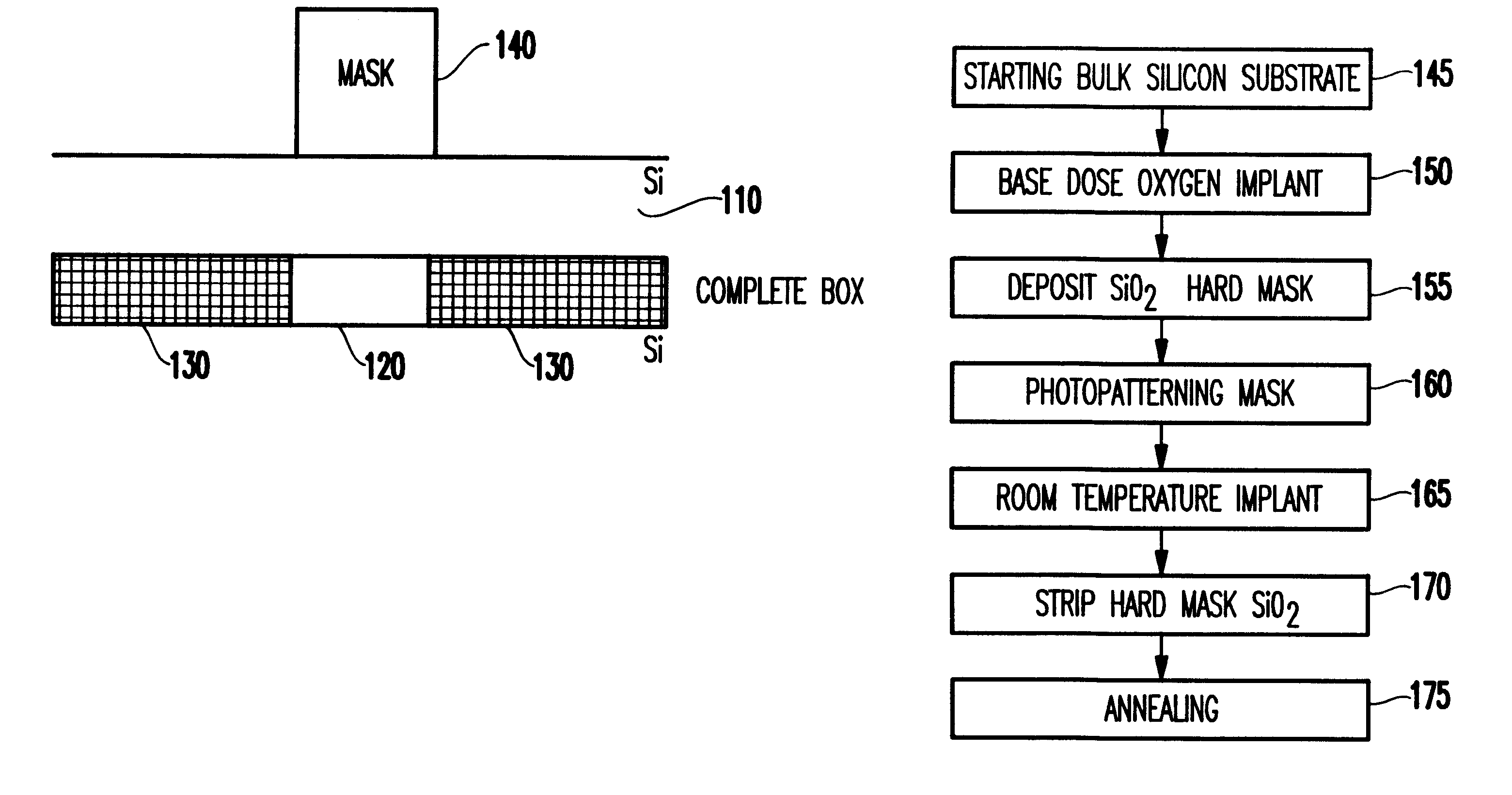
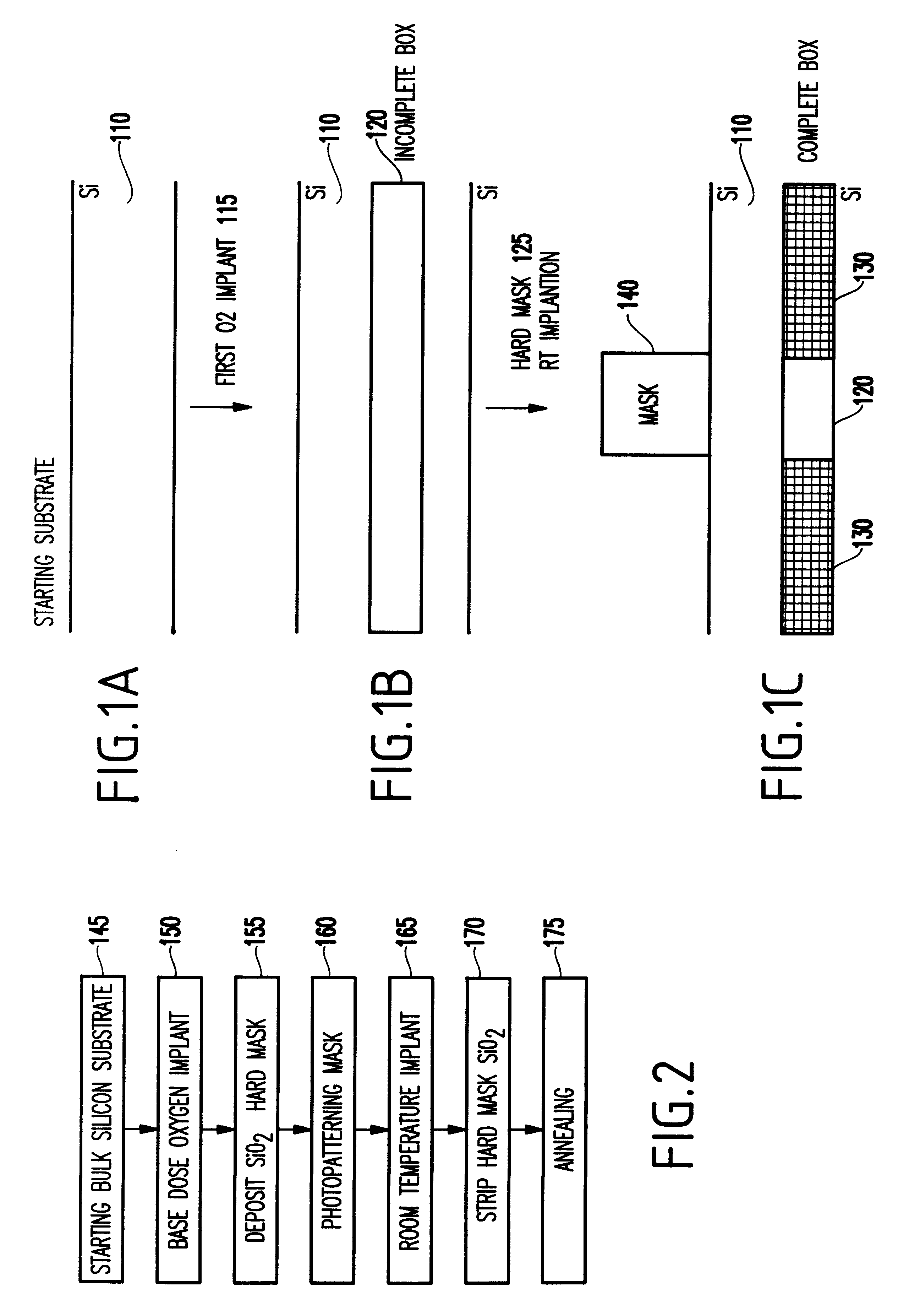
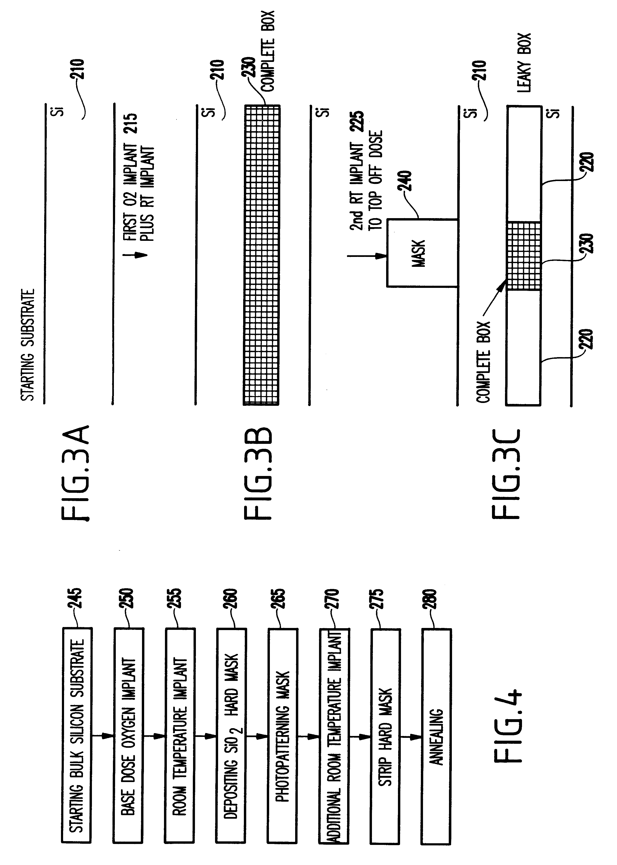
FIGS. 3A, 3B, 3C and FIG. 4 illustrate the present invention, which is an alternative desirable way to produce a body contact with a controllable BOX leakage by slightly adjusting the RT implant conditions until the desired leakage levels are achieved.

FIGS. 3A, 3B, and 3C show the structure of the second embodiment, more specifically a silicon substrate 210 undergoing a first oxygen implant and a room temperature implant 215 forming a complete BOX 230 in the silicon substrate layer 210 followed by a hard mask 240 and room temperature implantation 225. The complete structure is shown with the mask 240 on top of the silicon substrate layer 210 with a plurality of leaky BOX regions 220 shown sandwiching a complete BOX region 230.

The table below (Table 1) shows the dependence the BOX leakage has when the RT implant energy or dose is varied around the operating conditions typically used to produce a low leakage BOX. Table 1 shows that an increase in energy results in an ever-increasing B...

first embodiment

This second alternative sequence produces a body contact through a leaky BOX material only in the areas defined by the photopatterning of the hard mask. Because only slight modifications are made to the RT implant, any morphology problems inherent with the first embodiment are minimized. The amount of BOX oxidation during annealing is the same everywhere in this embodiment since it is exposed to both the base and the RT implant. The third ion implant is then used to create leakage with a minimal effect on topography.

FIGS. 5A, 5B, 5C and FIG. 6 illustrate a third embodiment of the present invention, which is an alternative method used to achieve the desirable results described in embodiment 2, without performing the RT implant twice. Here, a thin hard mask is used such that it only partially blocks the RT implant. The hard mask thickness and RT implant conditions are optimized to achieve the effect shown in Table 1, which once again shows how the BOX leakage increases as the RT impla...

third embodiment

FIGS. 5A, 5B, and 5C show the structure of the third embodiment, more specifically a silicon substrate 310 undergoing a first oxygen implant 315 forming an incomplete BOX 320 in the silicon substrate layer 310 followed by a thin hard mask pattern 341, and room temperature implantation 325. The complete structure is shown with a plurality of mask regions 341, on top of the silicon substrate layer 310 with a plurality of complete BOX regions 330 shown sandwiching an incomplete BOX region 320.

The sequence to achieve these results is detailed in FIG. 6, which shows the process of first starting 345 with a bulk silicon substrate 310, and then adding 350 a base dose oxygen implant 315 with predetermined parameters (dose 3.3E 17, energy 210 KeV, temperature 350.degree. C.). Then, a SiO.sub.2 hard mask 341 is deposited 355 using conventional masking techniques, at a thickness sufficient to block a subsequent room temperature implant from entering the silicon substrate. The thickness is "tun...


PUM


Abstract

A novel method for forming substrate contact regions on a SOI substrate without requiring additional space, and in order to provide lower diffusion capacitance. The method utilizes known semiconductor processing techniques. This method for selectively modifying the BOX region of a SOI substrate involves first providing a silicon substrate. Then, ion implanting the base using SIMOX techniques (e.g. O2 implant) is accomplished. Next, the substrate is photopatterned to protect the modified BOX region. Then, further ion implanting using a "touch-up" O2 implant is accomplished, thereby resulting in a good quality BOX as typically practiced. The final step is annealing the substrate. The area of the substrate, which had a mask present, would not receive the "touch-up" O2 implant (second ion implant), which in turn would result in a leaky BOX.

Description

1. Field of the InventionThe present invention generally relates to integrated circuit devices, and more particularly to an improved method for forming body contacts through the buried oxide region of a SOI semiconductor substrate.2. Description of the Related ArtIn buried layer devices known as silicon-on-insulator (SOI) devices, a buried insulation layer is formed beneath a thin surface silicon film. These devices have a number of potential advantages over conventional silicon devices (e.g., higher speed performance, higher temperature performance and increased radiation hardness).SOI technology leads to an appreciable simplification of manufacturing processes, an increase in integration density, improved behavior under high voltages, and low sensitivity to radiation, since the volume of monocrystalline silicon is low. Inherent in SOI technology are the various techniques of ion implantation.In one known technique of ion implantation, known by the acronym SIMOX, a very thin (0.1 m...

Claims


Application Information

Patent Timeline
IPC IPC(8): H01L21/70H01L21/762
CPCH01L21/76264H01L21/76267
Inventor GIEWONT, KENNETH J.ADLER, ERICGARG, NEENAHARGROVE, MICHAEL J.KOBURGER, III, CHARLES W.LEE, JUNEDONGSCHEPIS, DOMINIC J.YANG, ISABEL YING
Owner IBM CORP
Why Eureka
Try Eureka