Supercharge Your Innovation With Domain-Expert AI Agents!

Method of manufacturing photo interrupter including a positioning member with at least one positioning pin integrally provided with a connecting part, and photo interrupter manufactured thereby

a technology of positioning pins and photo interrupters, which is applied in the field of manufacturing photo interrupters, can solve the problems of increasing manufacturing costs due to increased manufacturing processes or the like, unavoidable increase in manufacturing costs due to increased manufacturing processes, and inability to provide positioning pins or the like on the cut surface, etc., and achieves the effect of large-scale manufacturing of photo interrupters and simple operation

Inactive Publication Date: 2011-10-25
CITIZEN ELECTRONICS CO LTD
View PDF5 Cites 1 Cited by
  • Summary
  • Abstract
  • Description
  • Claims
  • Application Information

AI Technical Summary

Benefits of technology

This method simplifies the manufacturing process, reduces costs, and ensures accurate positioning of photo interrupters on motherboards with minimal variation, enabling efficient and precise detection of object presence and absence.

Problems solved by technology

However, in the conventional photo interrupter as disclosed in Japanese Patent Application Publication No. 2000-12892, despite the accomplishment of a high accuracy in positioning of the photo interrupter on the motherboard by the positioning member provided on the frame, because the positioning member is formed separately from the frame, an extra process is required to make a plurality of positioning members and a troublesome operation is required to mount very small positioning members on the frame one by one.
Consequently, increased manufacturing cost due to increased manufacturing processes or the like is unavoidable.
Furthermore, in the conventional manufacturing method for the photo interrupter as disclosed in Japanese Patent No. 3640456, because a mounting surface of the photo interrupter, to be placed on a motherboard, is a surface cut by dicing, it is not possible to provide a positioning pin or the like on the cut surface.
Therefore, there is a problem that variation in a position of attaching the photo interrupter to the motherboard occurs, resulting in a photo interrupter of low accuracy.

Method used


Image

  • Method of manufacturing photo interrupter including a positioning member with at least one positioning pin integrally provided with a connecting part, and photo interrupter manufactured thereby
  • Method of manufacturing photo interrupter including a positioning member with at least one positioning pin integrally provided with a connecting part, and photo interrupter manufactured thereby
  • Method of manufacturing photo interrupter including a positioning member with at least one positioning pin integrally provided with a connecting part, and photo interrupter manufactured thereby

Examples


first embodiment

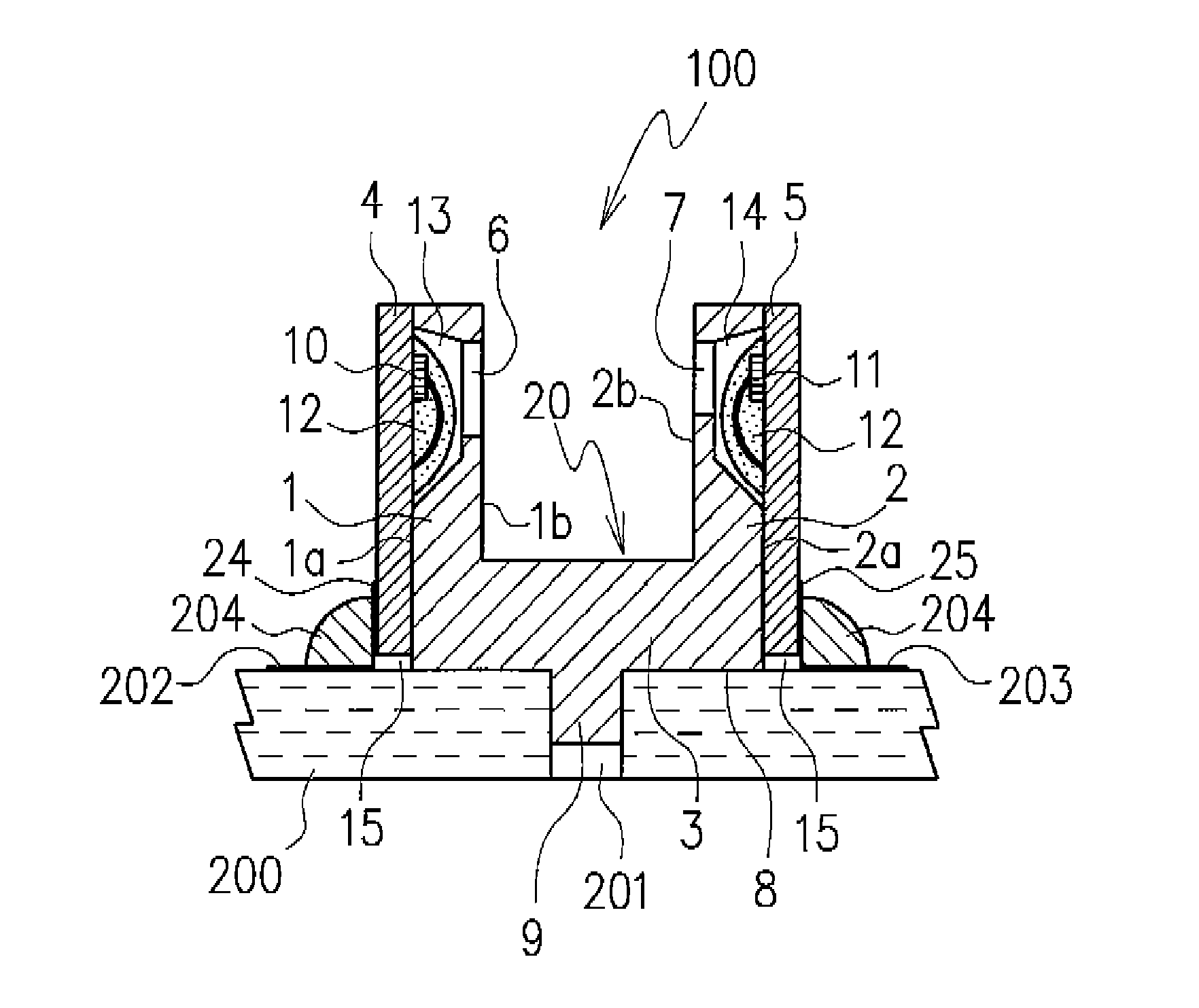
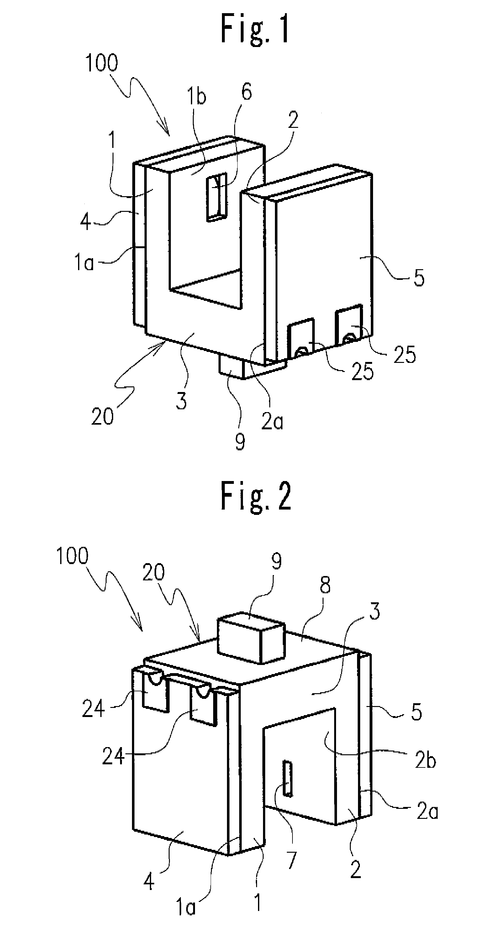
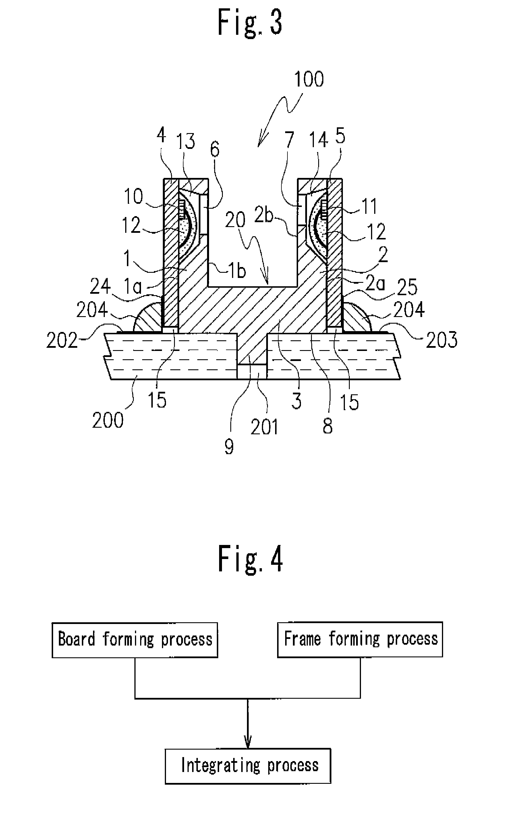
[0044]FIG. 1 to FIGS. 1 to 3 illustrates a first embodiment of a photo interrupter. A photo interrupter 100 having a frame that includes a first frame part 1 and a second frame part 2 that are disposed at an interval to face each other, a connecting part 3 integrally connecting the first frame part 1 and the second frame part 2, and a positioning member 6 integrally provided at a lower surface of the connecting part. The photo interrupter further includes a first board 4 provided at the first frame part, at least one light-emitting element mounted on the first board and its light-emitting surface exposed from an opening of the first frame part, a second board provided at the second frame part, and at least one light-receiving element mounted on the second board and its receiving surface exposed from an opening of the second frame part to face the at least one light-emitting element.

[0045]FIG. 4 illustrate a first embodiment of a method of manufacturing a photo interrupter and a phot...

second embodiment

[0064]Next, a method of manufacturing a photo interrupter, according to a second embodiment of the present invention and a photo interrupter manufactured by the same are described.

[0065]The manufacturing method in the second embodiment is configured to be capable of manufacturing a plurality of photo interrupters each having the aforementioned structure at a time. The manufacturing method basically includes a collecting board forming process, a frame assembly forming process, an integrating process and a separating process, which are described hereinafter. Here, it should be noted that an order of performing the collecting board forming process and the frame assembly forming process are not limited to the following order and may be set arbitrarily. In addition, the collecting board forming process includes a first collecting board forming process and a second collecting board forming process, in which an order thereof is not limited to the following order. Moreover, the integrating ...

third embodiment

[0096]Next, a photo interrupter according to a third embodiment of the present invention is described.

[0097]A frame assembly in the third embodiment differs from that in the second embodiment in shape only and is similar thereto in material, other structure and processes of manufacturing. Accordingly, mainly the differences are described below and common points having the same structure and operation are omitted.

[0098]FIG. 20 is a perspective view showing an appearance of a column frame as the frame assembly in the third embodiment.

[0099]In FIG. 20, the column frame 60 as the frame assembly has a structure in which a plurality of combined frames 40 are integrally connected in a column state, as separated by dashed-two dotted lines 43.

[0100]More specifically, the combined frames 40 are connected by abutting side surfaces of a first frame part 1, a second frame part 2 and a connecting part 3 connecting the first and second frame parts 1 and 2 of each of the combined frames 40. The con...


PUM

PropertyMeasurementUnit
shapeaaaaaaaaaa
thicknessaaaaaaaaaa
electricalaaaaaaaaaa

Abstract

A method of manufacturing a photo interrupter includes forming a frame including a first frame part and a second frame part which are disposed at an interval to be facing each other, mounting at least one light-emitting element on a first board and attaching the first board to the first frame part of the frame, mounting a light-receiving element on a second board and attaching the second board to the second frame part of the frame, the light-receiving element being mounted on the second board to be facing the light-emitting element so that the light-receiving element receives light emitted from the light-emitting element, and providing a positioning member on the frame by integrally forming the positioning member with the frame.

Description

CROSS-REFERENCE TO RELATED APPLICATION[0001]This application is based on and claims the priority benefit of Japanese Patent Application No. 2008-202596, filed on Aug. 6, 2008, the disclosure of which is incorporated herein by reference in its entirety.BACKGROUND OF THE INVENTION[0002]1. Field of the Invention[0003]The present invention relates to a method of manufacturing a photo interrupter to detect presence and absence or passing of an object with non-contact and a photo interrupter manufactured by the method of manufacturing.[0004]2. Description of the Related Art[0005]It is known that a photo interrupter is used in the field of information equipment, for example, in in-vehicle air conditioner panel operating switches, navigation control units, DVD recorders, digital cameras, printers, PC peripheral instruments or the like and can reliably detect a position or presence and absence or the like of an object with non contact by receiving light from a light-emitting element by a lig...

Claims


Application Information

Patent Timeline
Patent Type & Authority Patents(United States)
IPC IPC(8): G02B27/00
CPCG01V8/12H01L31/0203H01L31/167Y10T156/10H01L2224/48091Y10T156/1052H01L2924/00014
Inventor KINOSHITA, JO
Owner CITIZEN ELECTRONICS CO LTD
Features
  • R&D
  • Intellectual Property
  • Life Sciences
  • Materials
  • Tech Scout
  • Unparalleled Data Quality
  • Higher Quality Content
  • 60% Fewer Hallucinations
Learn More